EE-105 Electrical Engineering Material Science Oct-Nov 2025 paper solved: copper vs aluminium, magnetic force on a conductor and energy stored in a magnetic field
 Nookesh Karri ·· 56 min read

This post solves the AP SBTET C-23 DEEE first year electrical engineering material science question paper of October 2025 (EE-105, October/November 2025 board exam). It answers all 10 Part A questions and all 8 Part B questions. Each question first explains the theory in simple words, then gives a teacher’s exam answer sized to the marks, with a labelled figure for every question. You can open the original question paper PDF next to this page and check every question word for word.
Electrical Engineering Material Science question paper October 2025: pattern and syllabus units
The EE-105 paper of October 2025 follows the C-23 pattern: 3 hours, 80 marks, Part A with 10 questions of 3 marks (30 marks, all compulsory) and Part B with 8 questions of 10 marks, of which you answer any five (50 marks). No sums or circuit figures are printed.
Most Part B questions print a mark split: Q12 and Q15 to Q18 are “6+4”, Q13 is 6 and 4, and Q14 is “2+4+4”. The questions match the unit blueprint of the C-23 curriculum exactly: 2, 2, 1, 3 and 2 short questions, and 2, 2, 1, 2 and 1 essay questions from Units 1 to 5.
Part A instructions as printed on the paper (PART—A, 3×10=30):
Instructions : (1) Answer all questions.
(2) Each question carries three marks.
(3) Answers should be brief and straight to the point and shall not exceed five simple sentences.
Part B instructions as printed on the paper (PART—B, 10×5=50):
Instructions : (1) Answer any five questions.
(2) Each question carries ten marks.
(3) Answers should be comprehensive and the criteria for valuation is the content but not the length of the answer.
| Q no | Topic | Syllabus unit | Marks |
|---|---|---|---|
| 1 | Annealing | Unit 1 Conducting and Semiconducting Materials | 3 |
| 2 | Classification of semiconducting materials | Unit 1 | 3 |
| 3 | Factors affecting insulation resistance | Unit 2 Insulating and Dielectric Materials | 3 |
| 4 | Applications of dielectric materials | Unit 2 | 3 |
| 5 | Properties of ferromagnetic materials | Unit 3 Magnetic Materials | 3 |
| 6 | Field pattern of a straight conductor | Unit 4 Magnetic Effects of Electric Current and Electromagnetic Induction | 3 |
| 7 | Ampere’s work law | Unit 4 | 3 |
| 8 | SI units of B, reluctance and inductance | Unit 4 | 3 |
| 9 | Field pattern of unlike charges | Unit 5 Electrostatics and Capacitance | 3 |
| 10 | Dielectric strength | Unit 5 | 3 |
| 11 | Copper vs aluminium | Unit 1 | 10 |
| 12 | Formation of N-type semiconductor | Unit 1 | 6 + 4 |
| 13 | Conductors, insulators, semiconductors and band diagrams | Unit 2 | 6 + 4 |
| 14 | Electric dipole and polarization | Unit 2 | 2 + 4 + 4 |
| 15 | Hysteresis loop | Unit 3 | 6 + 4 |
| 16 | Mechanical force on a current carrying conductor | Unit 4 | 6 + 4 |
| 17 | Energy stored in a magnetic field | Unit 4 | 6 + 4 |
| 18 | Capacitance of a parallel plate capacitor | Unit 5 | 6 + 4 |
The paper has a few spelling slips (“aluminum”, “condoctors”, “dielectic”, “filed”, “fileld”); the questions below copy them exactly, and none of them changes what you must answer. Where the paper prints “6+4” with “neat diagrams”, this post reads it as 6 marks for the explanation or derivation and 4 marks for the diagrams.
My advice: in Part B, pick Q16, Q17, Q18, Q15 and Q13. The three derivations have fixed steps and standard figures, so every line you write can earn a mark. Q15 is one loop with six labelled points, and Q13 is a table plus three band diagrams. Leave Q11 unless you can write ten comparison rows from memory, because a missing row is a lost mark.
Almost every Part B topic here has come before. The N-type semiconductor, polarization, force on a conductor, energy stored and the parallel plate capacitor were all in the EE-105 paper of October 2024. Copper and aluminium, the band picture and the hysteresis loop were in the EE-105 paper of March 2025. You can see every EE-105 session on the Electrical Engineering Material Science subject page.
Q1. Define the process of annealing in metals. (3 marks)
Understand it first
- Heat treatment means heating a metal and cooling it in a controlled way. It changes the inside structure of the metal, not its shape.
- When a metal is hammered, rolled or drawn into wire, its tiny crystals get squeezed and twisted. This leaves internal stress inside. The metal becomes hard and springy, and it can crack.
- Annealing undoes this. You heat the metal to a set temperature, keep it there for some time, then let it cool very slowly.
- Keeping it hot is called soaking. It gives the crystals time to rearrange themselves.
- Slow cooling, often inside the switched-off furnace, lets the crystals settle without new stress.
- After annealing the metal is soft and ductile (easy to bend and draw into wire). Its electrical conductivity also improves a little.
Think of a crumpled bedsheet. Wash it and let it dry slowly on the line, and the creases relax. Annealing does the same for a metal’s crystals.
Where it is used: copper wire for motor and transformer windings is annealed so that it bends round the slots without cracking.
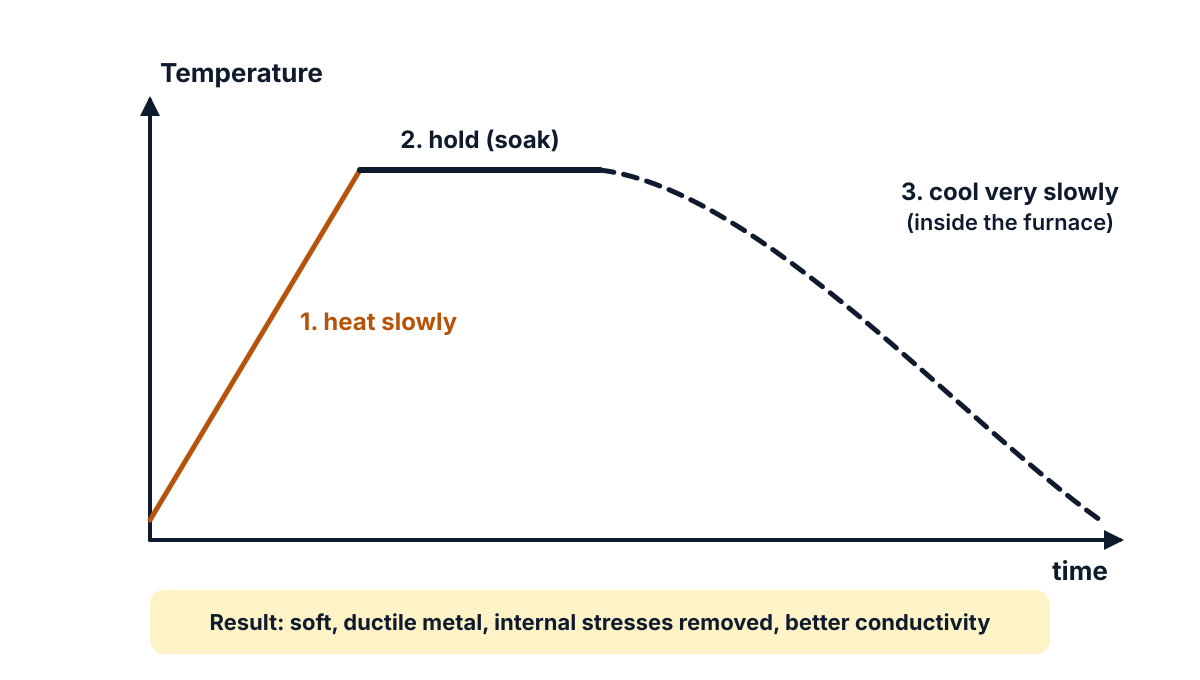
Figure Q1: annealing has three stages: heat, hold, and cool very slowly.
Exam answer (3 marks)
- Definition: annealing is a heat treatment process in which a metal is heated to a suitable temperature, held (soaked) at that temperature for some time, and then cooled very slowly, usually in the furnace itself.
- Effect: it makes the metal soft and ductile, removes internal stresses caused by cold working, and improves its electrical conductivity.
- Use: annealed copper is used for winding wires, flexible cables and house wiring, where the wire must bend easily.
Key points to write: heat to a set temperature; hold; cool slowly; soft, ductile, stress-free; annealed copper for windings.
Q2. Classify the semiconducting materials. (3 marks)
Understand it first
- A semiconductor is a material whose conductivity lies between that of a conductor and an insulator. Silicon (Si) and germanium (Ge) are the common ones.
- Both have four electrons in their outer shell. These are called valence electrons. Each atom shares them with four neighbours, and every shared pair is a covalent bond.
- A pure semiconductor is called intrinsic. In it, heat breaks a few bonds. Each broken bond gives one free electron and leaves one empty place called a hole. So the number of electrons equals the number of holes.
- Adding a tiny, controlled amount of another element is called doping. The added element is the impurity. A doped semiconductor is called extrinsic.
- Extrinsic semiconductors are of two kinds:
- P-type: doped with a trivalent impurity (3 valence electrons), such as boron, aluminium, gallium or indium. Holes are in the majority.
- N-type: doped with a pentavalent impurity (5 valence electrons), such as phosphorus, arsenic or antimony. Free electrons are in the majority.
An analogy: an intrinsic crystal is a class where only a few students are out of their seats. Doping is like letting in a group of extra students (N-type) or removing a few chairs so that empty seats appear (P-type).
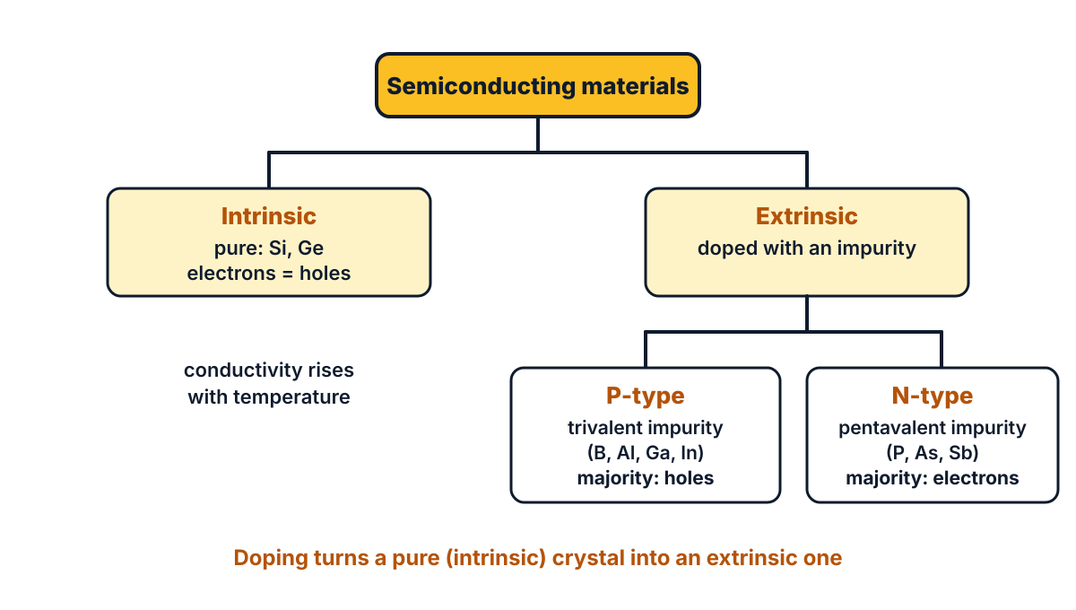
Figure Q2: semiconductors are intrinsic or extrinsic, and extrinsic ones are P-type or N-type.
Exam answer (3 marks)
Semiconducting materials are classified as follows:
- Intrinsic semiconductors: pure semiconductors such as silicon and germanium; the number of free electrons equals the number of holes, and conductivity is low at room temperature.
- Extrinsic semiconductors: semiconductors doped with a small amount of a suitable impurity to increase their conductivity.
- Types of extrinsic semiconductor: (i) P-type, doped with a trivalent impurity (boron, gallium, indium), holes are majority carriers; (ii) N-type, doped with a pentavalent impurity (phosphorus, arsenic, antimony), electrons are majority carriers.
Key points to write: intrinsic = pure, n = p; extrinsic = doped; P-type (trivalent, holes); N-type (pentavalent, electrons).
Q3. State the factors affecting insulation resistance. (3 marks)
Understand it first
- An insulator is a material that almost does not let current flow. PVC, rubber, mica and porcelain are examples.
- Still, a very small current always leaks through and over it. Insulation resistance is the resistance the insulation offers to this leakage current. It is very large, so it is measured in megohms (MΩ) with an instrument called a megger.
- High insulation resistance means the insulation is healthy. Low insulation resistance means current can leak to the body of a machine and give a shock or cause a fire.
- Things that lower it:
- Temperature: insulators behave opposite to metals. When they get hot, their resistance falls sharply.
- Moisture: water, and the salts dissolved in it, make easy paths for current. Damp insulation has much lower resistance.
- Dirt and dust: a dirty, wet surface lets current creep along the outside. This is surface leakage.
- Applied voltage: a higher voltage pushes more leakage current, and the measured resistance drops.
- Ageing: heat, sunlight and oxygen slowly crack and spoil insulation over the years.
Think of a raincoat. It keeps you dry when new and clean. When it is old, torn or soaked through, water gets in. Insulation fails in the same ways.
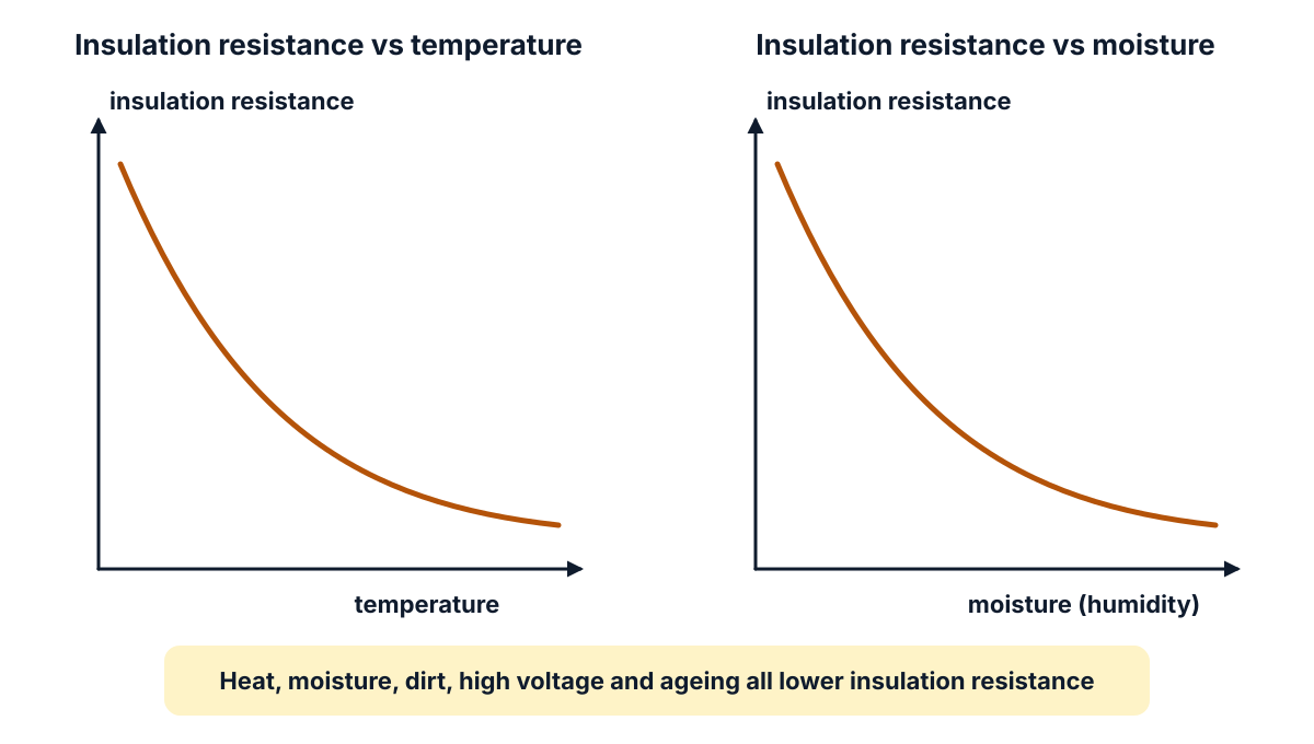
Figure Q3: insulation resistance falls quickly as temperature and moisture rise.
Exam answer (3 marks)
The factors affecting insulation resistance are:
- Temperature: insulation resistance decreases rapidly as temperature increases (insulators have a negative temperature coefficient of resistance).
- Moisture, humidity and dirt: absorbed moisture and a dirty, damp surface create leakage paths and reduce insulation resistance.
- Applied voltage and ageing: insulation resistance falls when the applied voltage is increased, and it falls as the insulation ages with heat, oxidation and mechanical damage.
Key points to write: temperature up, IR down; moisture and dirt lower IR; high voltage and ageing lower IR.
Q4. List the applications of dielectric materials. (3 marks)
Understand it first
- A dielectric is an insulating material that can store electric energy when it is placed in an electric field. Every dielectric is an insulator. We call it a dielectric when its job is to sit in an electric field, as between capacitor plates.
- The property that measures this is the relative permittivity (εr), also called the dielectric constant. It tells how many times more charge a capacitor stores with the dielectric than with vacuum between its plates.
- So dielectrics have two jobs:
- to insulate: keep current in its proper path (cables, transformers, insulators on poles);
- to store charge: increase the capacitance of capacitors.
- Common dielectrics are mica, paper, ceramic, glass, porcelain, PVC, rubber, transformer oil and air.
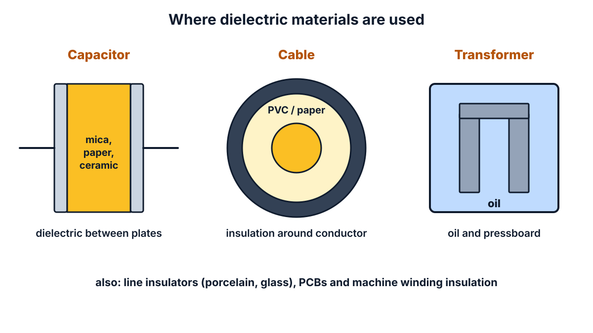
Figure Q4: three everyday places where dielectrics work: capacitors, cables and transformers.
Exam answer (3 marks)
Applications of dielectric materials:
- Capacitors: mica, paper, ceramic, polyester film and electrolytic oxide layers are used as the dielectric between the plates to increase capacitance.
- Cables and wires: PVC, rubber, polythene and impregnated paper are used as insulation for cables and wires.
- Machines, transformers and lines: transformer oil, pressboard and varnished paper insulate transformer windings; mica and glass tape insulate motor windings; porcelain and glass are used for line insulators and bushings.
Key points to write: capacitors (mica, paper, ceramic); cables (PVC, rubber, paper); transformers and machines (oil, pressboard, mica); line insulators (porcelain, glass).
Q5. State the properties of ferromagnetic materials. (3 marks)
Understand it first
- Magnetic materials are grouped by how they react to a magnet: diamagnetic (weakly pushed away), paramagnetic (weakly pulled) and ferromagnetic (strongly pulled).
- Ferromagnetic materials are the strongly magnetic ones: iron, nickel, cobalt and their alloys, such as silicon steel and alnico.
- Inside them, the tiny magnets of neighbouring atoms point the same way in small regions called domains. In an unmagnetised piece, different domains point in different directions, so they cancel.
- When a field is applied, the domains turn to line up with it. All the small magnets now add, so the material becomes a strong magnet.
- Relative permeability (μr) tells how much easier it is for magnetic flux to pass through the material than through air. For ferromagnetic materials it is very large.
- When all the domains are lined up, more field cannot add much more flux. This is saturation.
- If you heat a ferromagnetic material above a certain temperature, the domains break up and it becomes paramagnetic. That temperature is the Curie point.
An analogy: a crowd in a hall, each person facing a different way, is the unmagnetised iron. When a leader calls “face the stage”, everyone turns the same way. That is magnetisation.
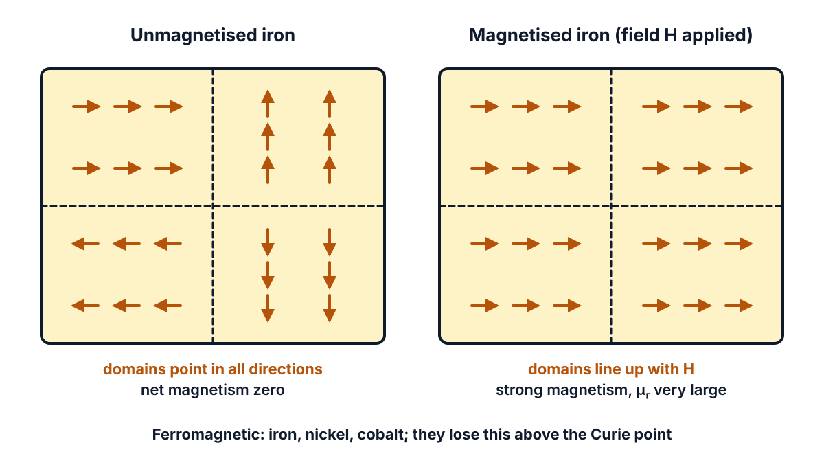
Figure Q5: in a field, the domains of a ferromagnetic material turn to point the same way.
Exam answer (3 marks)
Properties of ferromagnetic materials (iron, nickel, cobalt and their alloys):
- Strong magnetism: they are strongly attracted by a magnet; their relative permeability μr is very high (much greater than 1) and depends on the applied field.
- Hysteresis and saturation: they show hysteresis (B lags behind H), keep some magnetism after the field is removed (residual magnetism) and reach saturation at high fields.
- Domains and Curie point: their atomic magnets are grouped in domains; above the Curie point they lose their ferromagnetism and become paramagnetic.
Key points to write: strongly attracted; μr very large; hysteresis, residual magnetism, saturation; domains; Curie point.
Q6. Draw a neat sketch of magnetic field pattern due to a straight current carrying conductor. (3 marks)
Question (as printed): 6. Draw a neat sketch of magnetic field pattern due to a straight current carrying conductor.
Understand it first
- A magnetic field is the space around a magnet or a current where a magnetic force can be felt.
- We show a field with magnetic lines of force. They are imaginary lines. Their direction is the way a small north pole would move, and where they are close together the field is strong.
- Every current makes a magnetic field. For a long straight wire, the lines are concentric circles: circles with the wire at their common centre, in a plane at right angles to the wire.
- The circles are close together near the wire and spread out farther away, because the field gets weaker with distance.
- To show the wire end on, we use two signs:
- a dot (⊙) means the current comes out of the page towards you, like the point of an arrow;
- a cross (⊗) means the current goes into the page, like the tail feathers of an arrow.
- Right hand thumb rule: hold the wire in your right hand with the thumb pointing along the current. Your curled fingers show the direction of the lines.
- So current out of the page gives anticlockwise circles, and current into the page gives clockwise circles.
You can see this pattern in a lab: pass a strong current through a wire pushed through a card, sprinkle iron filings, and tap the card. The filings form rings.
Exam answer (3 marks)
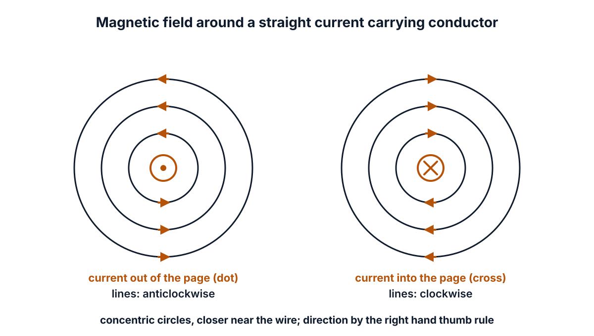
Figure Q6: the field of a straight conductor is a set of concentric circles; the direction reverses when the current reverses.
- Pattern: the magnetic lines of force around a straight current carrying conductor are concentric circles in a plane perpendicular to the conductor, with the conductor at the centre.
- Direction: given by the right hand thumb rule; anticlockwise for current out of the page (⊙) and clockwise for current into the page (⊗).
- Strength: the lines are crowded near the conductor and spread out with distance, showing that the field is strongest close to the conductor.
Key points to write: concentric circles; right hand thumb rule; ⊙ anticlockwise, ⊗ clockwise; strongest near the wire.
Q7. State Ampere’s work law. (3 marks)
Understand it first
- Magnetising force (H), also called field intensity, measures how strongly a current magnetises the space around it. Its unit is ampere-turns per metre (AT/m).
- Picture a single, free north pole of unit strength. Near a current, the field pushes on it.
- If you carry this pole once all the way round a closed path, the field does work on it, or you do work against the field.
- Ampere’s work law says this work depends only on the current that the path encloses. It does not depend on the shape or size of the path.
- For a path round a wire with current I, the work done is I. If the path encloses N turns each carrying I, the work done is N I, the magnetomotive force (mmf).
- In symbols: the sum of H × (small length of path) all round the path equals the current enclosed. Written as ∮H·dl = I.
- Use: it gives H easily for simple shapes. For a long straight wire, take a circle of radius r round it. H is the same all round, and the path length is 2πr. So H × 2πr = I, which gives H = I / (2πr).
Worked example: a long straight conductor carries I = 10 A. At r = 0.1 m from it, H = 10 / (2 × 3.1416 × 0.1) = 10 / 0.628 = 15.92 AT/m.
Picture walking once round a fountain. However wide or odd-shaped your path, you circle the same fountain. The work law counts the “fountain” of current inside, not the path.
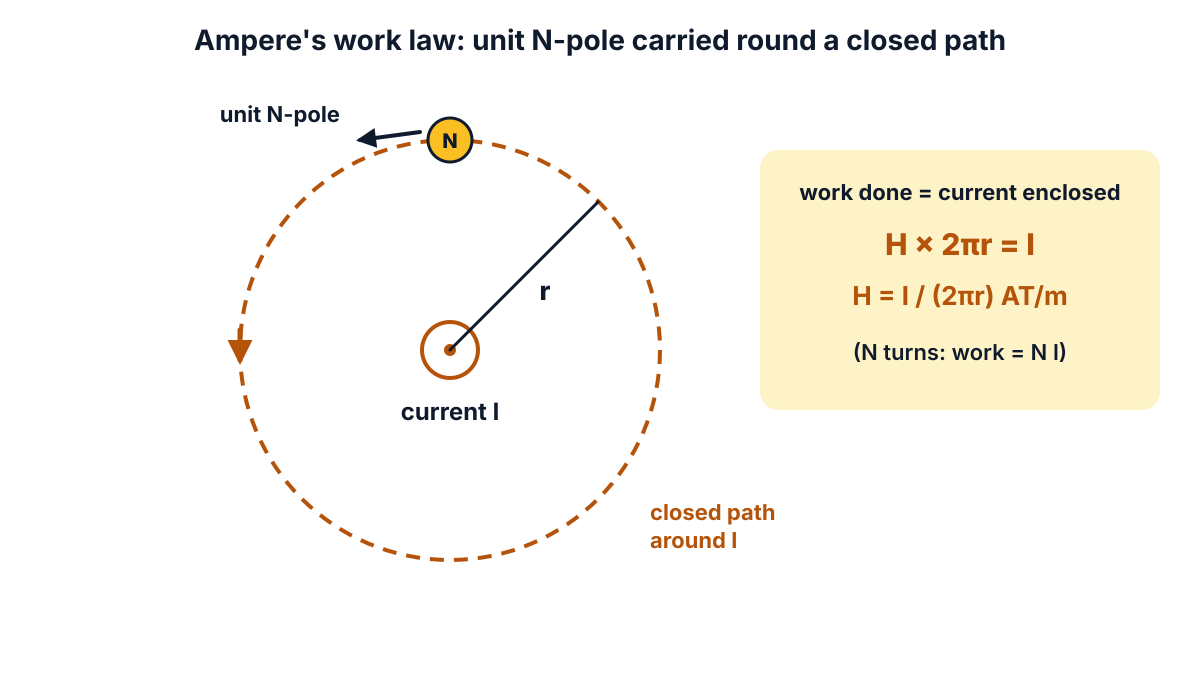
Figure Q7: carrying a unit N-pole once round the conductor needs work equal to the current enclosed.
Exam answer (3 marks)
- Statement: the work done in carrying a unit north pole once round any closed path in a magnetic field is equal to the current (in ampere-turns) enclosed by that path.
- Mathematical form: ∮H·dl = I; if the path encloses N conductors each carrying I, then ∮H·dl = N I = mmf.
- Application: for a long straight conductor, H × 2πr = I, so H = I / (2πr) AT/m; the law is also used to find H inside a solenoid and a toroid.
Key points to write: work on unit N-pole round a closed path = current enclosed; ∮H·dl = N I; H = I / (2πr).
Q8. Write the SI unit of (a) Magnetic Flux Density, (b) Reluctance (c) Inductance. (3 marks)
Question (as printed): 8. Write the SI unit of (a) Magnetic Flux Density, (b) Reluctance (c) Inductance.
Understand it first
- Magnetic flux (φ) is the total number of magnetic lines through a surface. Its unit is the weber (Wb).
- Magnetic flux density (B) is the flux passing through one square metre held at right angles to the flux: B = φ / A. So its unit is weber per square metre (Wb/m²). This unit has its own name: the tesla (T).
- Reluctance (S) is the opposition a magnetic circuit offers to flux. It is like resistance in an electric circuit. Flux = mmf / reluctance, so reluctance = mmf / flux. The mmf is in ampere-turns (AT) and flux in webers, so the unit is ampere-turns per weber (AT/Wb). Since turns have no unit, it is also written A/Wb, which equals H⁻¹ (per henry).
- Inductance (L) is the property of a coil that opposes any change of current in it. L = N φ / I, flux linkages per ampere. Its unit is the henry (H), which equals Wb/A.
- A coil has 1 henry if a current changing at 1 ampere per second induces 1 volt in it.
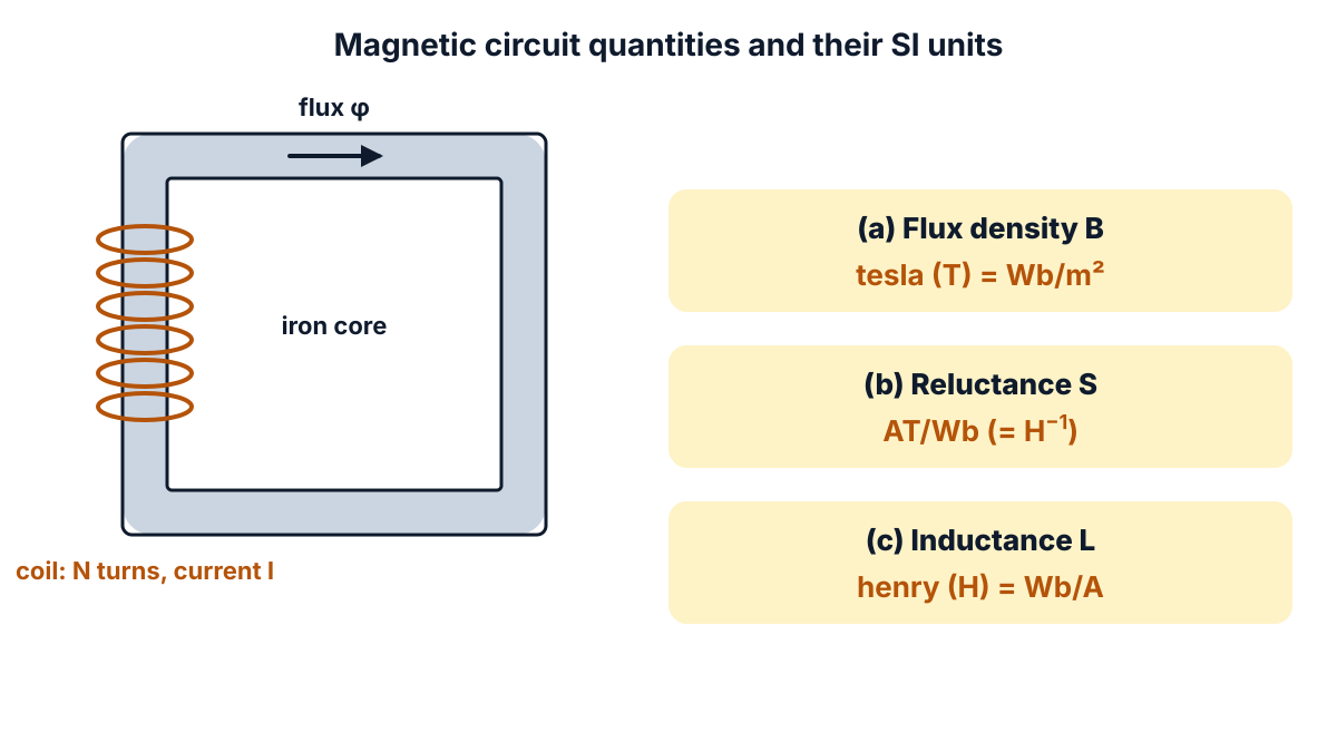
Figure Q8: the three quantities of a magnetic circuit and their SI units.
Exam answer (3 marks)
| Quantity | SI unit |
|---|---|
| (a) Magnetic flux density (B = φ / A) | tesla (T), equal to Wb/m² |
| (b) Reluctance (S = mmf / φ) | ampere-turn per weber (AT/Wb), also written A/Wb or H⁻¹ |
| (c) Inductance (L = N φ / I) | henry (H), equal to Wb/A |
Key points to write: B in tesla (Wb/m²); S in AT/Wb; L in henry.
Q9. Draw the neat sketch of electric field pattern due to unlike charges placed side by side. (3 marks)
Question (as printed): 9. Draw the neat sketch of electric field pattern due to unlike charges placed side by side.
Understand it first
- An electric field is the space around a charge where another charge feels a force.
- We draw it with electric lines of force. The direction of a line at any point is the way a small positive test charge would move there.
- Rules for these lines:
- they start on a positive charge and end on a negative charge;
- two lines never cross (at one point the force has only one direction);
- lines crowd together where the field is strong;
- like stretched elastic threads, they try to shorten and push each other sideways.
- Unlike charges are one positive and one negative charge. Lines leave the positive charge and curve round to end on the negative charge.
- The line straight between them is the shortest. The others bow outwards because neighbouring lines push each other apart.
- Because the lines try to shorten, they pull the two charges together. This is why unlike charges attract.
Picture many stretched rubber bands joining two balls. They pull the balls together, and they spread out sideways so they do not overlap.
Exam answer (3 marks)
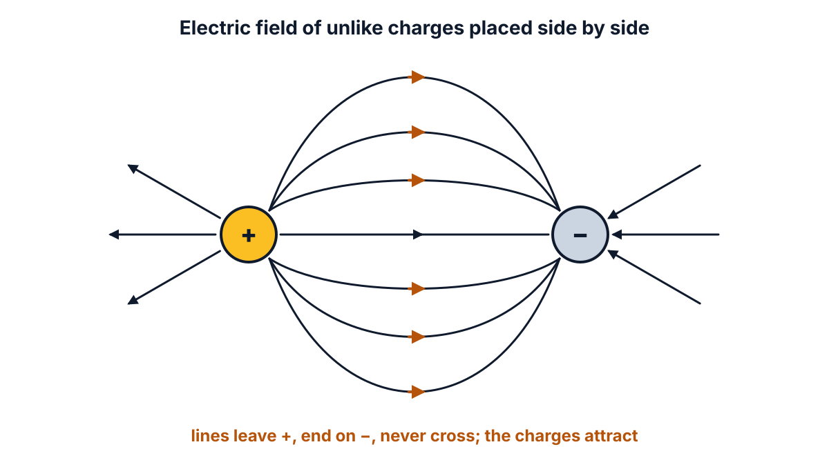
Figure Q9: lines of force start on the positive charge and end on the negative charge, showing attraction.
- Pattern: the lines of force start from the positive charge and end on the negative charge; the central line is straight and the others are curved outwards.
- Rules shown: the lines never intersect, and they are crowded in the region between the charges where the field is strongest.
- Result: the lines tend to contract along their length, so the two unlike charges attract each other.
Key points to write: lines from + to −; never cross; crowded between the charges; unlike charges attract.
Q10. Define dielectric strength of a material and state the units of dielectric strength of paper and vacuum. (3 marks)
Question (as printed): 10. Define dielectric strength of a material and state the units of dielectric strength of paper and vacuum.
Understand it first
- Every insulator has a limit. If you keep raising the voltage across it, at some point it suddenly lets a large current pass. It may spark, burn or get a hole punched through it. This is dielectric breakdown.
- The voltage at which this happens is the breakdown voltage.
- A thicker sheet can stand a higher voltage. So to compare materials fairly, we divide the breakdown voltage by the thickness.
- Dielectric strength is this ratio: the maximum voltage per unit thickness (electric field) a material can stand without breaking down. In one standard definition, it is “the maximum electric field that the material can withstand under ideal conditions without undergoing electrical breakdown”.
- Because it is volts divided by length, its unit is kilovolts per millimetre (kV/mm). You may also see kV/cm or MV/m. 1 kV/mm = 1 MV/m.
- The unit is the same for every material, including paper and vacuum. Only the value changes.
- The same open table gives about 40 to 60 kV/mm for waxed paper, and 20 to 40 kV/mm for a high vacuum (it depends on the shape of the electrodes). Ordinary dry air is much weaker, about 3 kV/mm. Values in books differ with the grade of paper and the test, so learn the unit first.
The question asks for the “units” of paper and vacuum. Both have the same unit, so give it, and add one value for each if you know them.
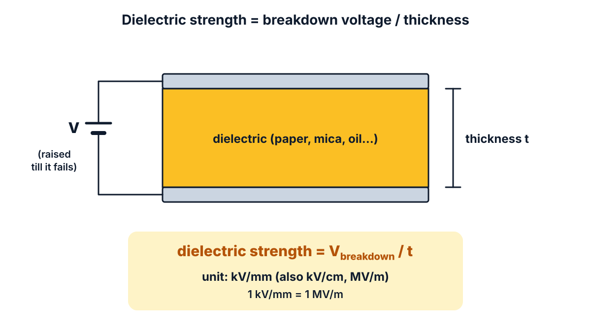
Figure Q10: dielectric strength is the breakdown voltage divided by the thickness of the dielectric.
Exam answer (3 marks)
- Definition: the dielectric strength of a material is the maximum voltage gradient (electric field) it can withstand without breakdown of its insulating property; dielectric strength = breakdown voltage / thickness, i.e. Vbreakdown / t.
- Unit: kilovolt per millimetre (kV/mm); it is also expressed in kV/cm or MV/m.
- Paper and vacuum: the unit is kV/mm for both paper and vacuum; typical values are about 40 to 60 kV/mm for waxed paper and about 20 to 40 kV/mm for high vacuum.
Key points to write: maximum voltage per unit thickness without breakdown; Vbreakdown / t; unit kV/mm for both paper and vacuum.
Q11. Compare copper with aluminum in any ten different aspects. (10 marks)
Understand it first
- Copper and aluminium are the two main low resistivity materials: materials that carry current with very little loss. Nearly every wire, winding and line uses one of them.
- Resistivity (ρ) is how strongly a material opposes current, for a standard piece 1 m long and 1 m² in cross-section. Low resistivity means a good conductor. Conductivity is its opposite.
- Density is mass per unit volume. A low density means a light conductor.
- Ductility is how easily a metal can be drawn into thin wire. Tensile strength is how much pull it can take before it breaks.
- The key numbers, from a standard resistivity table and the data pages for copper and aluminium:
- resistivity at 20 °C: copper (annealed) 1.72 × 10⁻⁸ Ω m, aluminium 2.82 × 10⁻⁸ Ω m;
- density: copper about 8.9 g/cm³, aluminium about 2.7 g/cm³;
- melting point: copper about 1085 °C, aluminium about 660 °C.
What the numbers tell you, step by step:
- Aluminium’s conductivity is 1.72 / 2.82 = 0.61 of copper’s, about 61%.
- For the same resistance and length, an aluminium conductor needs 2.82 / 1.72 = 1.64 times the cross-section of copper.
- Even so, it weighs only 1.64 × 2.70 / 8.935 = 0.495 of the copper one. That is about half.
- So copper wins where space is tight (machine windings, house wiring). Aluminium wins where weight and cost matter (overhead lines).
The properties and uses of each metal on its own were asked in the March 2025 paper. This time it is a side-by-side comparison, so write a table.
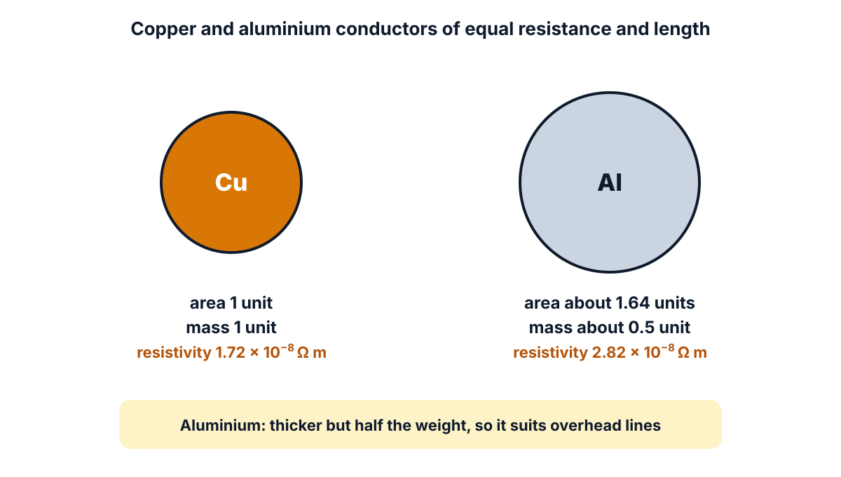
Figure Q11: for the same resistance, an aluminium conductor is thicker than a copper one but weighs about half as much.
Exam answer (10 marks)
Ten aspects, one mark each:
| No | Aspect | Copper | Aluminium |
|---|---|---|---|
| 1 | Resistivity at 20 °C | low, about 1.72 × 10⁻⁸ Ω m | higher, about 2.82 × 10⁻⁸ Ω m |
| 2 | Conductivity | very high (taken as 100%) | about 61% of copper |
| 3 | Density (weight) | heavy, about 8.9 g/cm³ | light, about 2.7 g/cm³ |
| 4 | Cross-section for the same resistance | smaller | about 1.64 times larger |
| 5 | Weight for the same resistance | more | about half of copper |
| 6 | Melting point | high, about 1085 °C | lower, about 660 °C |
| 7 | Mechanical strength and ductility | stronger, very ductile, withstands bending | weaker, soft; reinforced with steel (ACSR) for lines |
| 8 | Jointing | easily soldered, brazed and welded | difficult to solder; joined by clamps or special welding |
| 9 | Corrosion and cost | resists corrosion well; costly and less available | thin oxide film protects it; cheaper and plentiful |
| 10 | Applications | machine and transformer windings, house wiring, cables, bus bars, commutators | overhead lines (ACSR, AAAC), bus bars, cable sheaths, cage rotor bars |
Conclusion: copper is preferred where high conductivity in a small space is needed; aluminium is preferred where low weight and low cost matter, as in overhead lines.
Q12. Explain the formation of N-Type semi conductor with neat diagrams. (10 marks)
Understand it first
- Pure silicon has 4 valence electrons (outer electrons). In a crystal, each silicon atom shares one electron with each of its 4 neighbours. Each shared pair is a covalent bond. All 4 electrons are locked in bonds, so pure silicon has very few free electrons.
- Doping means adding a very small, controlled amount of another element to the pure crystal. The added atoms are the impurity.
- For N-type, the impurity is pentavalent: it has 5 valence electrons. Examples: phosphorus (P), arsenic (As) and antimony (Sb).
- The impurity atom takes the place of a silicon atom in the crystal. Four of its five electrons form covalent bonds with the four silicon neighbours.
- The fifth electron has no partner. It is held only very loosely. Even the small heat at room temperature frees it, and it wanders through the crystal as a free electron.
- Every impurity atom gives one free electron. That is why it is called a donor atom. After losing the electron, the donor atom becomes a fixed positive ion. It cannot move.
- Heat also breaks a few silicon bonds. These make some electron-hole pairs, as in pure silicon.
- So in N-type material, free electrons far outnumber holes. Electrons are the majority carriers and holes are the minority carriers. “N” stands for negative, the charge of the majority carriers. The crystal as a whole is still electrically neutral.
In the band picture:
- Electrons in a solid can only have energies inside certain ranges called energy bands. The valence band holds bonded electrons. The conduction band holds free electrons.
- The donor electrons sit at an energy level just below the conduction band, called the donor level.
- Only a tiny energy is needed to lift them into the conduction band, so at room temperature almost all of them are free.
Think of a class where every bench seats four, and every student has a bench partner. Now one bench gets a student who came with a fifth friend. The friend has no seat and wanders round the room. Each such bench adds one wanderer.
The same question, with one combined sketch, came in the EE-105 paper of October 2024. Here the split is 6 + 4: 6 marks for the explanation and 4 marks for the two diagrams.
Exam answer (10 marks)
(a) Formation of N-type semiconductor (6 marks)
- Definition: an N-type semiconductor is an extrinsic semiconductor formed by adding a small amount of pentavalent impurity to a pure (intrinsic) semiconductor such as silicon or germanium.
- Impurity used: pentavalent atoms such as phosphorus, arsenic or antimony, which have five valence electrons.
- Bonding: the impurity atom replaces a silicon atom in the crystal lattice; four of its five valence electrons form covalent bonds with the four neighbouring silicon atoms.
- Free electron: the fifth valence electron is not needed for bonding; it is loosely bound and becomes a free electron at room temperature.
- Donor: each impurity atom donates one free electron, so it is called a donor impurity; after giving up the electron it becomes an immobile positive ion.
- Carriers: free electrons are the majority carriers and holes (from thermally broken bonds) are the minority carriers; current is mainly due to electrons, and the crystal stays electrically neutral.
(b) Diagrams (4 marks)
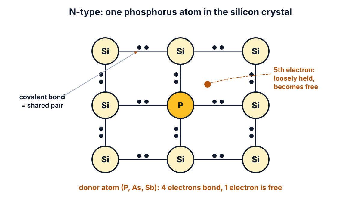
Figure Q12 (i): crystal lattice of N-type silicon; the fifth electron of the phosphorus atom becomes free.
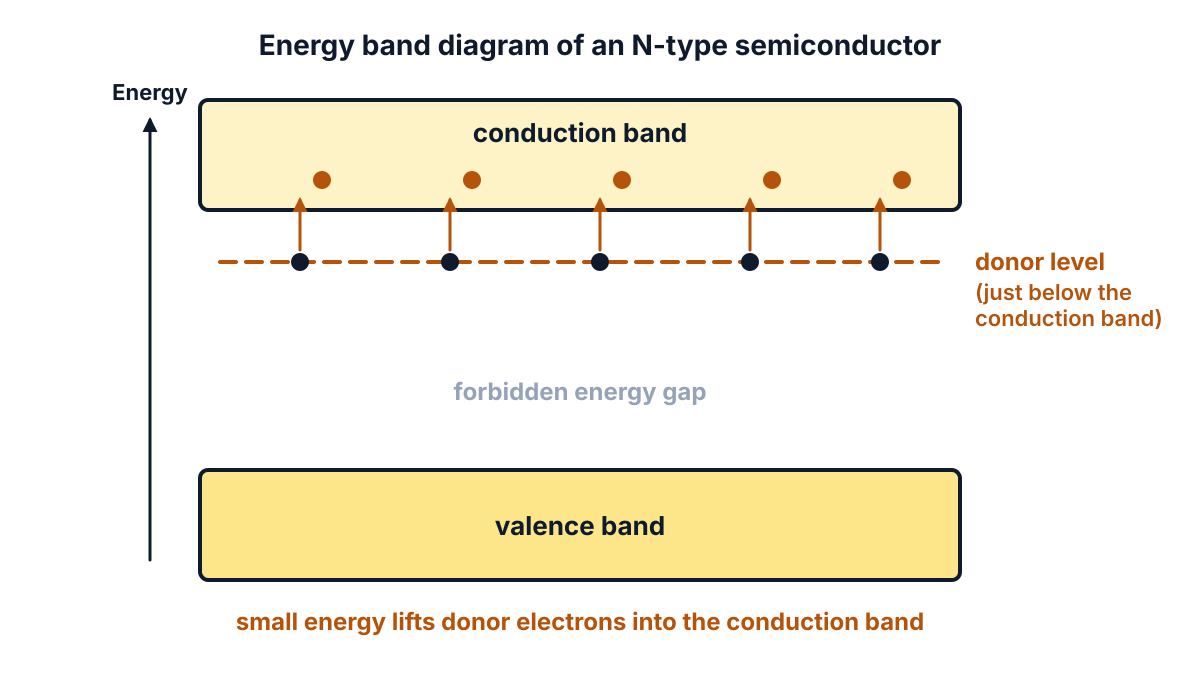
Figure Q12 (ii): energy band diagram of N-type material, with the donor level just below the conduction band.
- Lattice diagram: draw the silicon atoms in a grid with shared electron pairs, the pentavalent atom at the centre and its fifth electron shown free.
- Labels on the lattice: mark the covalent bonds, the donor atom (P, As or Sb) and the free electron.
- Band diagram: draw the conduction band, the valence band and the forbidden gap, with the donor level as a dashed line just below the conduction band.
- Labels on the band diagram: show arrows lifting donor electrons into the conduction band, and label the bands and the donor level.
Conclusion: adding a pentavalent impurity to pure silicon or germanium gives one free electron per impurity atom, so the N-type semiconductor conducts mainly by electrons.
Q13. (a) Distinguish among conductors, insulators and semiconductors any six different aspects. (10 marks)
Question (as printed): 13. (a) Distinguish among conductors, insulators and semiconductors any six different aspects. 6
(b) Draw neat sketches of energy band diagram of condoctors, semi conductors and insulators. 4
Understand it first
- Electrons in a solid can only have energies inside certain ranges. These ranges are called energy bands.
- The valence band holds the outer electrons that are tied to their atoms. They cannot carry current.
- The conduction band holds electrons that are free to move. Only these carry current.
- Between the two bands there may be a range of energy that no electron can have. This is the forbidden energy gap, Eg. It is measured in electron volts (eV), a tiny unit of energy.
- The size of the gap decides what the material is:
- Conductor: the two bands overlap. There is no gap, so plenty of electrons are always free. Example: copper.
- Semiconductor: there is a small gap, about 1 eV. Band gap tables give about 1.1 eV for silicon and 0.7 eV for germanium. Heat lifts a few electrons across.
- Insulator: there is a wide gap, 5 eV or more. Almost no electron can cross it. Example: mica, glass.
- Temperature coefficient of resistance tells whether resistance rises or falls when the material is heated. In a conductor, hot atoms shake more and get in the electrons’ way, so resistance rises (positive coefficient). In a semiconductor, heat frees more electrons, so resistance falls (negative coefficient).
Think of a building with two floors. People can move freely only on the upper floor. In a conductor, a wide ramp joins the floors. In a semiconductor, there is a short ladder that a few people climb when they have energy. In an insulator, there is a tall wall with no ladder.
The paper prints “semiconductors any six different aspects” without “in”, and “condoctors” in part (b); read them as “in any six different aspects” and “conductors”. The split is printed: 6 marks for (a) and 4 marks for (b).
Exam answer (10 marks)
(a) Distinction in six aspects (6 marks)
| No | Aspect | Conductor | Insulator | Semiconductor |
|---|---|---|---|---|
| 1 | Energy gap | no gap; bands overlap | large, 5 eV or more | small, about 1 eV (Si 1.1 eV, Ge 0.7 eV) |
| 2 | Conductivity | very high | negligible | in between, can be controlled |
| 3 | Free electrons at room temperature | very large number | almost none | few |
| 4 | Temperature coefficient of resistance | positive | negative | negative |
| 5 | Current carriers | free electrons | practically none | free electrons and holes |
| 6 | Examples | copper, aluminium, silver | mica, glass, rubber, PVC | silicon, germanium |
(b) Energy band diagrams (4 marks)
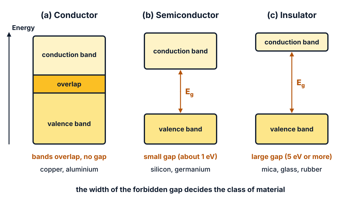
Figure Q13: band diagrams of a conductor, a semiconductor and an insulator; the width of the gap Eg decides the class.
- Conductor: the conduction band and valence band overlap; there is no forbidden gap.
- Semiconductor: a narrow forbidden gap of about 1 eV separates the conduction band from the valence band.
- Insulator: a wide forbidden gap of 5 eV or more separates the two bands.
- Labels: draw an energy axis, and mark the conduction band, valence band and Eg on each sketch.
Conclusion: the width of the forbidden energy gap decides whether a solid is a conductor, a semiconductor or an insulator.
Q14. What is an electric dipole? Explain polarization in dielectic materials with neat diagrams. (10 marks)
Question (as printed): 14. What is an electric dipole? Explain polarization in dielectic materials with neat diagrams. 2+4+4
Understand it first
- An atom has a positive nucleus at its centre and a cloud of negative electrons round it. Normally the centre of the electron cloud sits exactly on the nucleus, so the atom shows no charge from outside.
- An electric dipole is a pair of equal and opposite charges, +q and −q, separated by a small distance d.
- The dipole moment (p) measures how strong a dipole is: p = q × d. Its unit is coulomb metre (C m). It is drawn as an arrow from −q to +q.
- Now place a dielectric between two charged plates. The electric field E pushes the positive nucleus one way and pulls the electron cloud the other way.
- The centres of positive and negative charge separate a little. Each atom becomes a tiny dipole. This is an induced dipole.
- All these dipoles line up with the field. Inside the material, the + end of one dipole sits next to the − end of the next, so they cancel.
- But at the two faces they do not cancel. A layer of negative charge appears on the face next to the positive plate, and a layer of positive charge on the face next to the negative plate. These are bound charges. They cannot flow away like free charges.
- This whole effect, lining up of dipoles and appearance of bound charges, is called polarization.
- The bound charges set up their own field opposite to E. So the net field inside the dielectric becomes weaker. For the same voltage, the plates can hold more charge. That is why a dielectric increases capacitance and why its relative permittivity εr is greater than 1.
- Some molecules, like water, are dipoles even without a field. In a field they simply turn to line up. So polarization can come from electrons shifting, ions shifting, or ready-made dipoles turning.
Picture a row of people holding hands, each one leaning a little to the right when a wind blows. Inside the row, every hand meets a hand. Only the two people at the ends have a free hand. The bound charges are those “free hands” at the faces.
The same topic, asked without the dipole part, came in the October 2024 paper. This paper splits it 2+4+4: 2 marks for the dipole, 4 for explaining polarization and 4 for the diagrams.
Exam answer (10 marks)
(a) Electric dipole (2 marks)
- Definition: an electric dipole is a system of two equal and opposite point charges, +q and −q, separated by a small distance d.
- Dipole moment: p = q × d, in coulomb metre (C m); it is a vector directed from −q to +q.
(b) Polarization in dielectric materials (4 marks)
- Displacement of charges: when a dielectric is placed in an electric field E, the positive nuclei are displaced along E and the electron clouds opposite to E, so each atom or molecule becomes an induced dipole; polar molecules turn to align with E.
- Alignment and bound charges: the dipoles line up with the field; inside they cancel, but a negative bound charge appears on the surface facing the positive plate and a positive bound charge on the surface facing the negative plate.
- Definition: this alignment of dipoles and appearance of bound surface charges in a dielectric under an electric field is called polarization; the polarization P is the dipole moment per unit volume (C/m²).
- Effect: the bound charges produce a field opposite to the applied field, so the net field inside is reduced; hence the dielectric increases capacitance and its relative permittivity εr is greater than 1.
(c) Diagrams (4 marks)
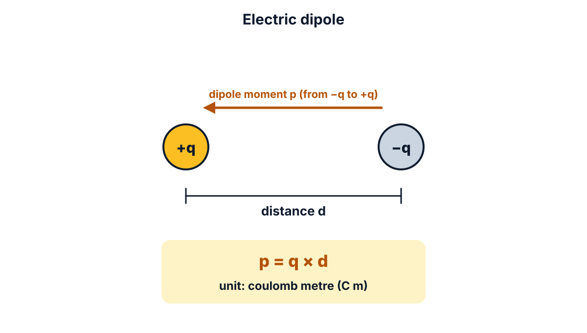
Figure Q14 (i): an electric dipole with dipole moment p = q × d.
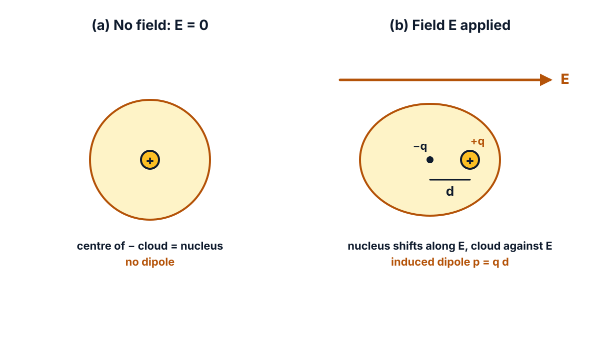
Figure Q14 (ii): an atom becomes an induced dipole when a field is applied.
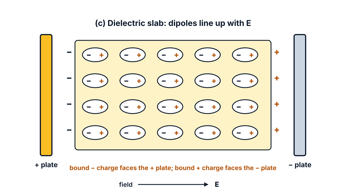
Figure Q14 (iii): a polarized dielectric between charged plates, with bound charges on its faces.
- Dipole sketch: +q and −q a distance d apart, with p marked from −q to +q.
- Atom sketch: an atom with no field (cloud centred on the nucleus) beside an atom in a field E (nucleus and cloud separated by d).
- Slab sketch: a dielectric between a positive and a negative plate, with dipoles lined up along E.
- Labels: mark the field direction, the plates and the bound charges on the two faces of the slab.
Conclusion: an electric field turns the atoms of a dielectric into aligned dipoles; the bound surface charges reduce the field inside, which is why dielectrics increase capacitance.
Q15. Explain hysteresis loop in magnetic material with neat diagrams. (10 marks)
Understand it first
- Magnetising force (H) is the cause: it is set by the current in the coil, H = N I / l, in ampere-turns per metre (AT/m), where l is the length of the magnetic path.
- Flux density (B) is the effect: how much magnetism the iron actually gets, in tesla.
- If you raise H, then lower it, B does not come back down the same way. B always lags behind H. This lagging is called hysteresis, from a Greek word meaning “to lag behind”.
- Take an iron ring with a coil on it, and a circuit that lets you raise, lower and reverse the current. Plot B against H as you go once round:
- o to a: start from an unmagnetised ring. Raise H. B rises along a curve until the iron saturates at a.
- a to b: lower H to zero. B does not fall to zero. The amount left is the residual magnetism or retentivity, Br.
- b to c: reverse the current and raise H the other way. At c, B becomes zero. The reverse H needed is the coercive force or coercivity, Hc.
- c to d: raise the reverse H further. The iron saturates in the opposite direction at d.
- d to e to f to a: lower H to zero (B = −Br at e), then raise it positive (B = 0 at f, H = +Hc), and on to a.
- The closed curve a b c d e f a is the hysteresis loop.
- Turning the domains back and forth takes energy, which turns into heat. The energy lost in one cycle, per unit volume, equals the area of the loop. This is hysteresis loss.
- Steinmetz found a formula for it: Wh = η Bmax1.6 f V watts, where η is the Steinmetz coefficient, f the frequency and V the volume of iron.
Push a heavy door against a stiff spring hinge, then let go. It does not swing back exactly to where it was. Some of your push was used up in the hinge as friction and heat. The loop area is that “used-up push”.
The C-23 syllabus asks you to draw and explain this loop. It also came, with soft and hard materials, in the March 2025 paper.
Exam answer (10 marks)
(a) Explanation (6 marks)
- Hysteresis: the lagging of flux density B behind magnetising force H in a magnetic material, when the material is taken through a cycle of magnetisation, is called hysteresis.
- Initial magnetisation (o to a): when H is increased from zero, B increases along the curve oa and the material reaches saturation at a.
- Residual magnetism (a to b): when H is reduced to zero, B does not become zero; the value ob = Br is the residual magnetism (retentivity).
- Coercive force (b to c): to make B zero, H must be reversed; the reverse value oc = Hc is the coercive force (coercivity).
- Reverse cycle (c to d to e to f to a): increasing H in the reverse direction gives negative saturation at d; reducing H to zero leaves −Br at e; applying positive H of value of = +Hc makes B zero at f, and further increase brings the material back to a, completing the loop abcdefa.
- Hysteresis loss: the area of the loop represents the energy lost as heat per cycle per unit volume; it is given by Steinmetz’s equation Wh = η Bmax1.6 f V watts, and is kept small by using materials with a narrow loop, such as silicon steel.
(b) Diagrams (4 marks)
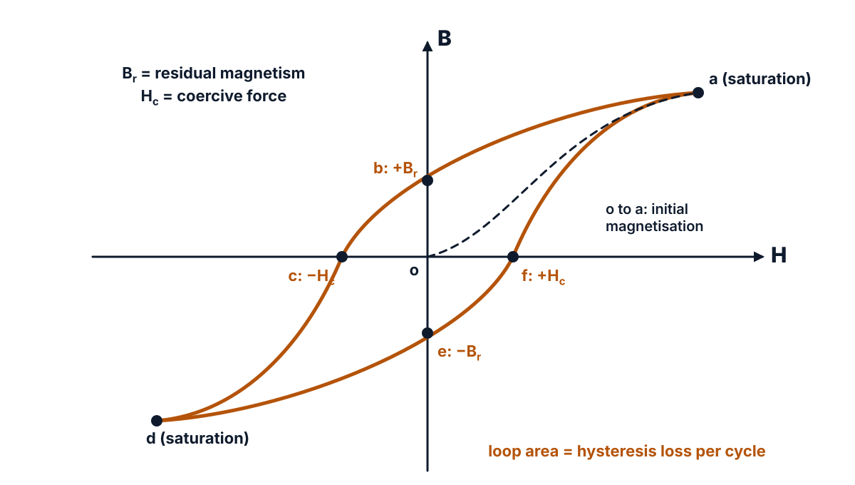
Figure Q15 (i): the hysteresis loop, with residual magnetism Br and coercive force Hc marked.
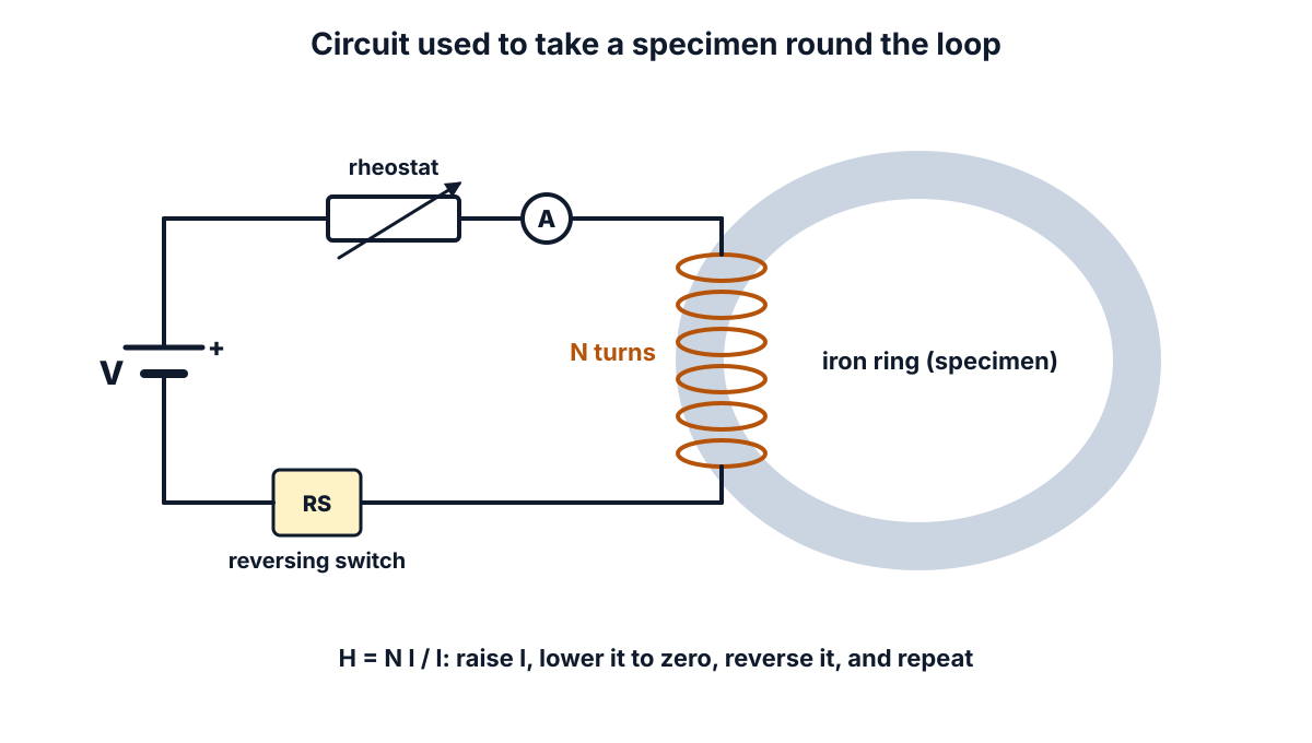
Figure Q15 (ii): the circuit used to take an iron ring through a full cycle of magnetisation.
- Axes: draw H on the horizontal axis and B on the vertical axis, with the origin o.
- Loop: draw the initial curve oa and the closed loop abcdefa, symmetrical about the origin.
- Labels: mark saturation points a and d, +Br and −Br at b and e, and −Hc and +Hc at c and f.
- Circuit: draw the battery, rheostat, ammeter and reversing switch connected to a coil of N turns on the iron ring specimen.
Conclusion: the hysteresis loop shows the residual magnetism, the coercive force and, through its area, the hysteresis loss of a magnetic material.
Q16. Explain the mechanical force produced in a current carrying conductor placed in magnetic filed with neat diagrams. (10 marks)
Question (as printed): 16. Explain the mechanical force produced in a current carrying conductor placed in magnetic filed with neat diagrams. 6+4
Understand it first
- Magnetic flux density (B) tells how strong a magnetic field is, in tesla (T). A strong magnet between two poles gives a nearly uniform field: straight, parallel, evenly spaced lines from N to S.
- A current-carrying wire makes its own circular field round it (Q6).
- Put the wire in the main field. On one side of the wire, its circular field points the same way as the main field, so the two add and the lines crowd together. On the other side they point opposite ways, so they cancel and the field is weak.
- Magnetic lines behave like stretched rubber bands. The crowded, bent lines try to straighten. They push the wire from the strong side towards the weak side. This push is the mechanical force. Because of the bent lines, this picture is often called the catapult field.
- Fleming’s left hand rule gives the direction. Stretch the thumb, first finger and second finger of the left hand at right angles to each other. Point the First finger along the Field and the seCond finger along the Current. The thuMb then shows the Motion (force).
- How big is the force? Experiments show it grows with the field B, the current I and the length l of wire inside the field.
- The angle matters too. Split B into two parts:
- B cos θ along the wire. It is like pushing a pencil along its length on a table. Nothing happens. No force.
- B sin θ at right angles to the wire. Only this part pushes the wire sideways.
- So F = B I l sin θ newtons. It is greatest (F = B I l) when the wire is at right angles to the field, and zero when the wire lies along the field.
Worked example: B = 0.6 T, I = 5 A, l = 0.4 m. At θ = 90°, F = 0.6 × 5 × 0.4 = 1.2 N. At θ = 30°, sin 30° = 0.5, so F = 1.2 × 0.5 = 0.6 N. At θ = 0°, F = 0.
Where it is used: this force turns every electric motor and moves the pointer of a moving coil meter.
This derivation came in the October 2024 paper as well.
Exam answer (10 marks)
(a) Explanation and expression (6 marks)
- Interaction of fields: when a current carrying conductor is placed in a magnetic field, its own circular field combines with the main field; on one side the fields add and become strong, on the other side they oppose and become weak.
- Origin of force: the distorted lines of force try to straighten like stretched elastic threads, so they push the conductor from the strong-field side to the weak-field side; this is the mechanical force on the conductor.
- Direction: the force acts at right angles to both the conductor and the field, and its direction is given by Fleming’s left hand rule (first finger: field, second finger: current, thumb: motion).
- Resolving the field: consider a conductor of length l metres carrying I amperes at an angle θ to a uniform field of flux density B tesla; of the components B cos θ (along the conductor) and B sin θ (perpendicular to it), only B sin θ produces force.
- Magnitude: the force is directly proportional to B sin θ, to I and to l, so F = k B I l sin θ, and k = 1 in SI units; hence F = B I l sin θ newtons.
- Special cases: F is maximum, F = B I l, when θ = 90° (conductor perpendicular to the field), and F = 0 when θ = 0° (conductor along the field); this force is the principle of the electric motor.
(b) Diagrams (4 marks)
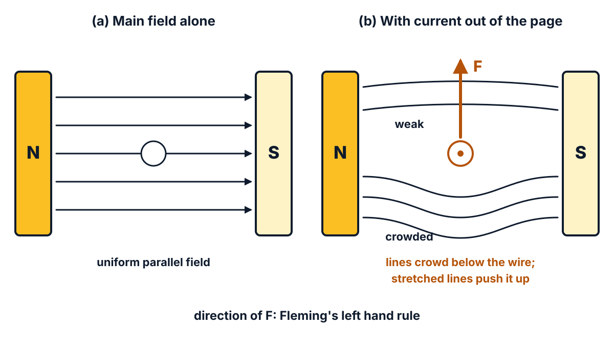
Figure Q16 (i): the main field alone, and the distorted field with current in the conductor; the wire is pushed from the crowded side to the weak side.
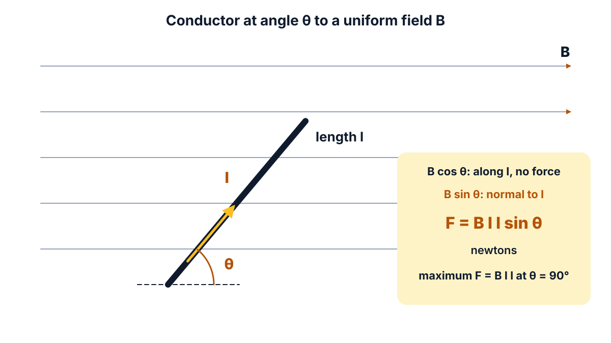
Figure Q16 (ii): only the component B sin θ, at right angles to the conductor, produces the force F = B I l sin θ.
- Main field: draw uniform parallel lines from the N pole to the S pole.
- Distorted field: draw the conductor (⊙ or ⊗) between the poles, with lines crowded on one side, weak on the other, and the force F from strong to weak.
- Angle diagram: draw the conductor at angle θ to the lines of B, with I, l and θ marked.
- Components: show B cos θ along the conductor (no force) and B sin θ normal to it (gives F).
Answer: F = B I l sin θ newtons; maximum F = B I l at θ = 90°, zero at θ = 0°; direction by Fleming’s left hand rule.
Q17. Derive an expression for energy stored in a magnetic fileld with neat diagrams. (10 marks)
Question (as printed): 17. Derive an expression for energy stored in a magnetic fileld with neat diagrams. 6+4
Understand it first
- Self inductance (L) is the property of a coil that opposes any change of current in it. Its unit is the henry (H).
- When you switch on a coil, the current does not jump to its final value I at once. It rises from zero.
- While the current is rising, the flux in the coil is rising too. A changing flux induces an emf in the coil itself. This self-induced emf is e = L di/dt.
- By Lenz’s law, this emf opposes the rise of current. It acts like a back-push.
- To keep the current rising, the supply must do work against this back emf. This work is not lost as heat. It is stored in the magnetic field of the coil.
- When you switch off, the field collapses and gives this energy back. That is why a spark jumps at the switch when an inductive circuit is opened.
- Doing the sum: in a small time dt, the energy given is (emf × current × time) = L (di/dt) × i × dt = L i di. Adding up all these small bits as i goes from 0 to I gives W = ½ L I².
- On a graph of flux linkage (L i) against current (i), the line is straight. The energy is the area of the triangle under it: ½ × base × height = ½ × I × L I = ½ L I².
Worked example: a coil with L = 0.4 H carries I = 5 A. Then I² = 25 and W = ½ × 0.4 × 25 = 5 J.
It is like pushing a heavy cart to get it moving. The cart resists at first. Your work is stored as the cart’s motion, and it comes back when the cart is stopped. Inductance is the “heaviness”, and current is the “speed”: W = ½ L I² looks just like ½ m v².
The same derivation came in both the October 2024 and the March 2025 papers.
Exam answer (10 marks)
(a) Derivation (6 marks)
- Set-up: consider a coil of self inductance L henry connected to a d.c. supply through a switch S; when S is closed, the current rises from zero to its final value I amperes.
- Self-induced emf: at any instant, when the current is i and rising at the rate di/dt, a self-induced emf e = L di/dt is set up which opposes the rise of current (Lenz’s law).
- Power: to drive current against this emf, the supply must provide power p = e × i = L i di/dt watts.
- Energy in time dt: the energy supplied in a small time dt is dW = p dt = L i (di/dt) dt = L i di joules.
- Total energy: as the current rises from 0 to I, the total energy is W = ∫₀ᴵ L i di = L [i²/2]₀ᴵ = ½ L I².
- Result: this energy is stored in the magnetic field of the coil and is returned when the current falls to zero: W = ½ L I² joules.
(b) Diagrams (4 marks)
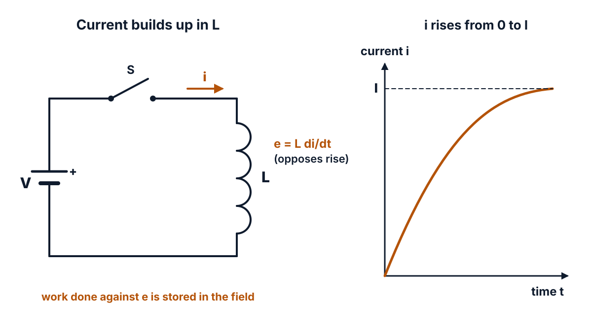
Figure Q17 (i): the circuit and the rise of current from 0 to I in the inductor.
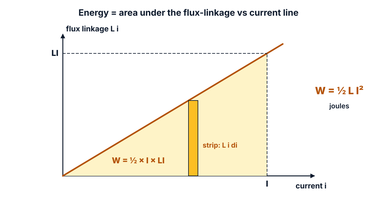
Figure Q17 (ii): the energy stored is the area of the triangle under the flux linkage line: ½ × I × L I.
- Circuit: draw the battery V, switch S and coil L in series, with the current i and the opposing emf e = L di/dt marked.
- Current growth curve: draw i against time t, rising from zero and levelling off at I.
- Energy graph: draw flux linkage L i against i as a straight line through the origin, with a thin strip L i di shaded.
- Area: shade the triangle up to I and mark its area ½ × I × L I = ½ L I².
Answer: W = ½ L I² joules, stored in the magnetic field of the coil.
Q18. Derive an expression for capacitance of a parallel plate capacitor with neat diagrams. (10 marks)
Question (as printed): 18. Derive an expression for capacitance of a parallel plate capacitor with neat diagrams. 6+4
Understand it first
- A capacitor is two conducting plates separated by an insulator (the dielectric). It stores electric charge.
- Capacitance (C) is the charge stored per volt: C = Q / V. Its unit is the farad (F). One farad is very large, so we often use microfarad (µF) and picofarad (pF).
- In a parallel plate capacitor, two flat plates of area A face each other at a small distance d. When a voltage V is applied, one plate gets +Q and the other −Q.
- Between the plates the field is uniform: straight, parallel, equally spaced lines from + to −.
- The derivation chains five simple ideas:
- Electric flux (ψ): the charge Q sends out flux equal to itself, ψ = Q coulombs.
- Flux density (D): flux per square metre of plate, D = Q / A.
- Field intensity (E): D = ε₀εrE, so E = D / (ε₀εr). Here ε₀ is the permittivity of free space, 8.854 × 10⁻¹² F/m from the CODATA value, and εr is the relative permittivity of the dielectric.
- Voltage: in a uniform field, voltage = field × distance, so V = E d.
- Capacitance: C = Q / V.
- Putting them together gives C = ε₀εrA / d.
- So capacitance goes up with a larger plate area, a smaller gap and a dielectric with higher εr.
Worked example: A = 0.05 m², d = 1 mm = 0.001 m, air (εr = 1). C = 8.854 × 10⁻¹² × 0.05 / 0.001 = 4.427 × 10⁻¹⁰ F = 442.7 pF. Fill the gap with a dielectric of εr = 4, and C = 4 × 442.7 = 1770.8 pF, about 1.77 nF.
A capacitor is like a water tank. A wider tank (bigger A) holds more. A dielectric is like a tank wall that stretches, so the same pressure (voltage) holds more water (charge).
The same derivation was asked in the October 2024 paper.
Exam answer (10 marks)
(a) Derivation (6 marks)
- Set-up: consider two parallel plates, each of area A m², separated by a distance d metres, with a dielectric of relative permittivity εr between them; a voltage V gives charges +Q and −Q on the plates.
- Electric flux: the flux between the plates is ψ = Q coulombs.
- Flux density: D = ψ / A = Q / A C/m².
- Field intensity: since D = ε₀εrE, the field between the plates is E = D / (ε₀εr) = Q / (ε₀εrA) V/m (uniform, fringing neglected).
- Potential difference: for a uniform field, V = E × d = Q d / (ε₀εrA) volts.
- Capacitance: C = Q / V = Q / [Q d / (ε₀εrA)], so C = ε₀εrA / d farads; for air, C = ε₀A / d.
(b) Diagrams (4 marks)
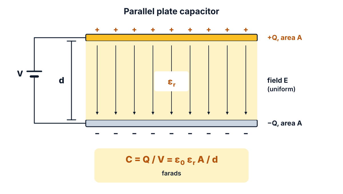
Figure Q18 (i): a parallel plate capacitor with plate area A, spacing d, dielectric εr and a uniform field E.
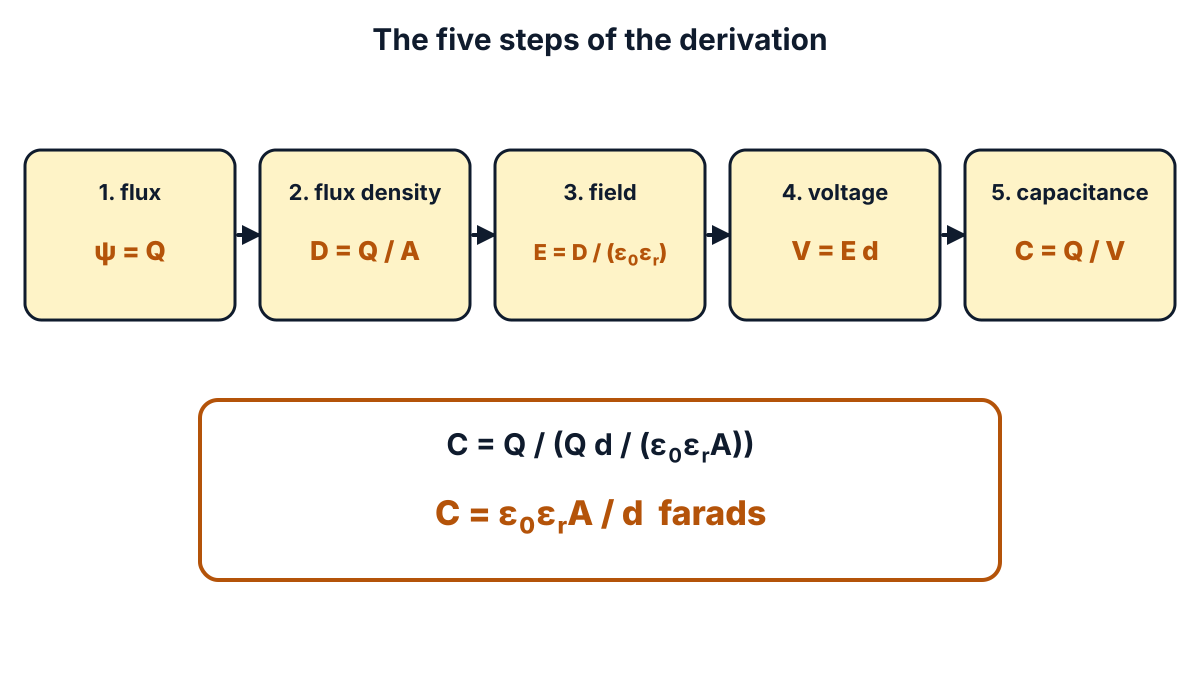
Figure Q18 (ii): the chain of the derivation, from flux to capacitance.
- Plates: draw two parallel plates connected to a supply V, the upper marked +Q and the lower −Q.
- Dimensions: mark the plate area A and the separation d.
- Field: draw uniform, parallel lines of force from the + plate to the − plate and label E.
- Dielectric: shade the space between the plates and label it εr.
Answer: C = ε₀εrA / d farads (C = ε₀A / d for air).
FAQ
Which units carry the most marks in the EE-105 October 2025 paper?
Unit 4 (magnetic effects of electric current and electromagnetic induction) carries 29 marks: Q6, Q7, Q8, Q16 and Q17. Units 1 and 2 carry 26 marks each, Unit 5 carries 16 and Unit 3 carries 13. These totals include the Part B choice, so they add up to 110, the unit weightage of the C-23 syllabus.
Which five Part B questions should I choose in this paper?
Q16, Q17, Q18, Q15 and Q13 are the safest five. The three derivations and the hysteresis loop have fixed steps and standard figures, and Q13 is a table plus three band diagrams. Q11 needs ten comparison rows from memory, and Q12 and Q14 need careful diagrams, so take them only if you have practised them.
What does ‘6+4’ after a Part B question mean?
It splits the 10 marks. In this paper it is read as 6 marks for the explanation or derivation and 4 marks for the neat diagrams the question asks for. So write about six clear points or steps, and draw two labelled figures. Q14 is split 2+4+4: 2 marks for the dipole, 4 for polarization and 4 for the diagrams.
Are there spelling mistakes in this paper?
Yes. The paper prints ‘aluminum’, ‘condoctors’, ‘dielectic’, ‘filed’ and ‘fileld’ (for field). None of them changes the question. Read them as aluminium, conductors, dielectric and field, and answer normally.
What should I write for the dielectric strength of paper and vacuum in Q10?
The unit is the same for both: kilovolts per millimetre (kV/mm), also written kV/cm or MV/m. One open table gives about 40 to 60 kV/mm for waxed paper and 20 to 40 kV/mm for high vacuum, depending on the electrodes. Write the unit first; values differ between books, so give one only if your teacher taught it.
Sources
- AP SBTET C-23 DEEE EE-105 question paper, Oct-Nov 2025
- C-23 Curriculum, Diploma in Electrical and Electronics Engineering, SBTET AP
- Reference books (C-23 syllabus):
- K. Padmanabham: Electronic Components, Laxmi Publications
- Electrical Engineering Materials, NITTTR Publications
- B.K. Agarwal: Introduction to Engineering Materials, Tata McGraw Hill
- Ian P. Jones: Material Science for Electrical and Electronic Engineers, Oxford
- B.L. Theraja: Electrical Technology Vol. 1, S. Chand
- Electrical resistivity and conductivity: resistivity table at 20 °C (Wikipedia)
- Copper: physical properties (Wikipedia)
- Aluminium: physical properties (Wikipedia)
- Band gap: values for silicon, germanium and diamond (Wikipedia)
- Dielectric strength: definition and table of values (Wikipedia)
- Vacuum electric permittivity, CODATA recommended value (NIST)
Writes and reviews the SBTET EEE Papers solutions: AP SBTET diploma question papers answered step by step from the prescribed syllabus.