EE-105 Electrical Engineering Material Science Oct-Nov 2024 paper solved: N-type semiconductor, dielectric polarization and parallel plate capacitor
 Nookesh Karri ·· 49 min read

This post solves the AP SBTET C-23 DEEE first year electrical engineering material science question paper of 2024 (EE-105, October/November 2024 board exam). It answers all 10 Part A questions and all 8 Part B questions. Each question first explains the theory in simple words, then gives a teacher’s exam answer sized to the marks, with a labelled figure wherever the textbook answer has one. You can open the original question paper PDF next to this page and check every question word for word.
Electrical Engineering Material Science question paper 2024: pattern and syllabus units
The EE-105 paper of October 2024 follows the C-23 pattern: 3 hours, 80 marks, Part A with 10 questions of 3 marks (30 marks, all compulsory) and Part B with 8 questions of 10 marks, of which you answer any five (50 marks). It is a pure theory paper with no sums and no figures printed. The questions match the unit blueprint of the C-23 curriculum exactly: 2, 2, 1, 3 and 2 short questions, and 2, 2, 1, 2 and 1 essay questions from Units 1 to 5.
Part A instructions as printed on the paper (PART—A, 3×10=30):
Instructions : (1) Answer all questions.
(2) Each question carries three marks.
(3) Answers should be brief and straight to the point and shall not exceed five simple sentences.
Part B instructions as printed on the paper (PART—B, 10×5=50):
Instructions : (1) Answer any five questions.
(2) Each question carries ten marks.
(3) Answers should be comprehensive and the criteria for valuation is the content but not the length of the answer.
| Q no | Topic | Syllabus unit | Marks |
|---|---|---|---|
| 1 | Applications of carbon | Unit 1 Conducting and Semiconducting Materials | 3 |
| 2 | P-type vs N-type semiconductors | Unit 1 | 3 |
| 3 | Classes of insulation by temperature | Unit 2 Insulating and Dielectric Materials | 3 |
| 4 | Factors affecting dielectric loss | Unit 2 | 3 |
| 5 | Classification of magnetic materials | Unit 3 Magnetic Materials | 3 |
| 6 | Coefficient of coupling | Unit 4 Magnetic Effects of Electric Current and Electromagnetic Induction | 3 |
| 7 | Fleming’s left hand rule | Unit 4 | 3 |
| 8 | Faraday’s laws of electromagnetic induction | Unit 4 | 3 |
| 9 | Gauss theorem | Unit 5 Electrostatics and Capacitance | 3 |
| 10 | Electric flux density | Unit 5 | 3 |
| 11 | Manganin and Constantan | Unit 1 | 10 |
| 12 | Formation of N-type semiconductor | Unit 1 | 10 |
| 13 | Impregnated paper and PVC | Unit 2 | 10 |
| 14 | Polarization of a dielectric | Unit 2 | 10 |
| 15 | Types of magnetic materials | Unit 3 | 10 |
| 16 | Force on a current carrying conductor, F = BIl sin θ | Unit 4 | 10 |
| 17 | Energy stored in a magnetic field, W = ½LI² | Unit 4 | 10 |
| 18 | Capacitance of a parallel plate capacitor | Unit 5 | 10 |
My advice: in Part B, pick Q18, Q16, Q17, Q12 and Q14. Each one has fixed steps and a standard figure, so every point you write can earn a mark. Q11 and Q13 look easy, but they are pure memory lists; choose them only if you have learnt the properties by heart. You can see every EE-105 session together on the Electrical Engineering Material Science subject page.
Q1. List any three applications of Carbon. (3 marks)
Understand it first
- Carbon is a non-metal. In electrical work it is used mainly in the form of graphite, a soft, black, slippery form of carbon.
- Carbon conducts electricity, but much less well than copper. So it is a high resistivity material. Resistivity is how strongly a material opposes current, for a standard size of piece.
- Carbon has three more useful habits. It does not melt easily, it is self-lubricating (it slides smoothly), and its resistance falls a little as it gets hotter.
Think of a pencil. The pencil “lead” is graphite. It leaves a mark because it slides off in thin layers. The same slipperiness lets a carbon brush rub on a spinning motor part without wearing it out.
Where each property is used:
- Slides smoothly and conducts: brushes of DC motors and generators.
- Opposes current and is cheap: carbon resistors.
- Stands very high temperature: electrodes of arc lamps, arc furnaces and arc welding.
- Does not react with the chemicals in a cell: the centre rod of a dry cell.
Exam answer (3 marks)
- Brushes: carbon brushes are used in DC motors and generators to carry current to and from the rotating commutator. Carbon slides smoothly and does not damage the commutator.
- Resistors: carbon is used to make carbon composition and carbon film resistors for electronic circuits.
- Electrodes: carbon electrodes are used in arc lamps, arc furnaces, arc welding and as the positive rod of dry cells, because carbon stands very high temperatures.
Key points to write: brushes of DC machines; carbon resistors; electrodes of arc lamps, arc furnaces and dry cells.
Q2. Distinguish between P and N Type semiconductors in any three aspects. (3 marks)
Understand it first
- A semiconductor conducts better than an insulator but worse than a conductor. Silicon (Si) and germanium (Ge) are the common ones.
- Pure silicon has 4 electrons in its outer shell. These are valence electrons. In the crystal, every one of them is locked in a bond, so pure silicon conducts poorly.
- Doping means adding a very small amount of another element, called an impurity, to make the crystal conduct better.
- A hole is the empty place left in a bond when an electron is missing. It behaves like a positive charge that can move.
- Majority carriers are the charge carriers present in large numbers. Minority carriers are the few of the other kind.
Two kinds of doping give two kinds of semiconductor:
- Add a trivalent impurity (3 valence electrons: boron, aluminium, gallium). One bond around each impurity atom is short of an electron. That leaves a hole. This is P-type (P for positive holes).
- Add a pentavalent impurity (5 valence electrons: phosphorus, arsenic, antimony). One electron is left over and becomes free. This is N-type (N for negative electrons).
An analogy: a cinema hall with exactly one seat per person. Send a few people out (P-type) and you get empty seats that “move” as people shift along. Bring in extra people with no seats (N-type), and they wander in the aisle. Both make movement possible.
Exam answer (3 marks)
| Aspect | P-type semiconductor | N-type semiconductor |
|---|---|---|
| Impurity added | Trivalent impurity (boron, aluminium, gallium) | Pentavalent impurity (phosphorus, arsenic, antimony) |
| Majority carriers | Holes (electrons are minority carriers) | Free electrons (holes are minority carriers) |
| Name of impurity atom | Acceptor, because it accepts an electron | Donor, because it donates an electron |
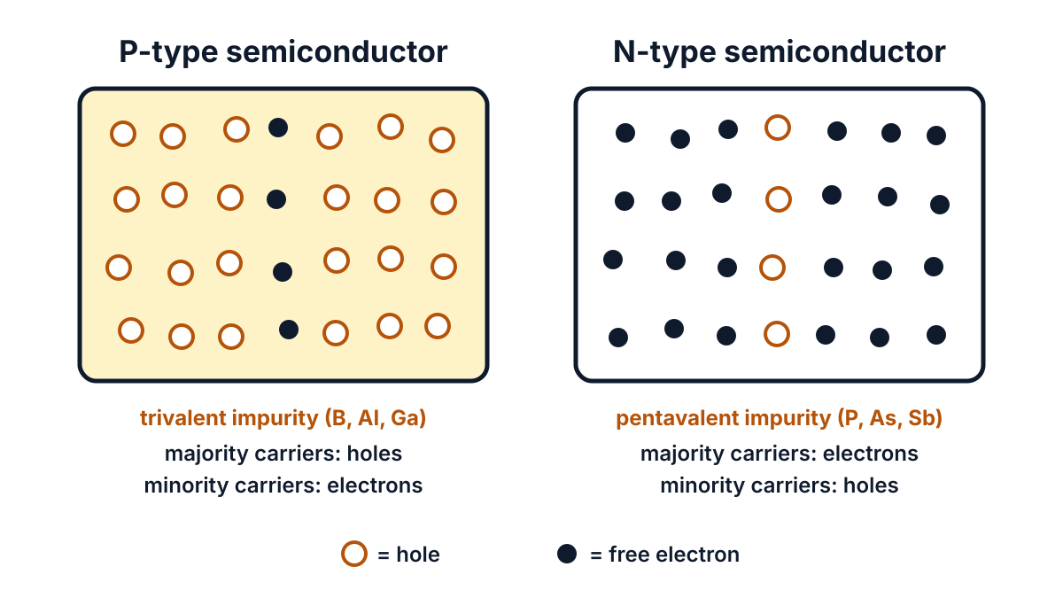
Figure Q2: in P-type material holes are the majority carriers; in N-type material free electrons are the majority carriers.
Key points to write: trivalent vs pentavalent impurity; holes vs electrons as majority carriers; acceptor vs donor.
Q3. Classify insulating materials on the basis of temperature. (3 marks)
Understand it first
- An insulating material is one that does not let current pass. Its job is to keep current inside the wire.
- Heat slowly damages insulation. Paper turns brown and brittle, varnish cracks, rubber hardens.
- So every insulating material has a maximum safe working temperature. Above it, the insulation ages fast and finally fails.
- Engineers group materials into thermal classes by this temperature. Each class has a letter.
Think of cooking pots. A plastic bowl is fine for cold food, a steel pot for the stove, and a clay pot for the oven. You choose by the heat it must face. A motor designer does the same with insulation: a hot motor winding needs a higher class.
The classes rise in steps: Y, A, E, B, F, H, C. Class Y is the coolest (plain cotton and paper). Class C is the hottest (mica, porcelain, glass with no organic binder). The insulation class table used today also adds higher classes such as 200 °C and 220 °C. For the C-23 exam, learn Y to C.
Exam answer (3 marks)
- Basis: insulating materials are classified by the maximum temperature at which they can work safely for a long time.
- Classes:
| Class | Maximum temperature | Typical materials |
|---|---|---|
| Y | 90 °C | Cotton, silk, paper (not impregnated) |
| A | 105 °C | Cotton, silk, paper impregnated with varnish or immersed in oil |
| E | 120 °C | Polyurethane, epoxy resin, polyester films |
| B | 130 °C | Mica, glass fibre, asbestos with suitable binders |
| F | 155 °C | Mica, glass fibre with heat-stable binders such as epoxy |
| H | 180 °C | Silicone rubber, mica and glass fibre with silicone binders |
| C | Above 180 °C | Mica, porcelain, glass, quartz (no organic binder) |
- Use: the class decides the temperature rise allowed in a machine; for example, a hotter motor winding needs class F or H insulation.
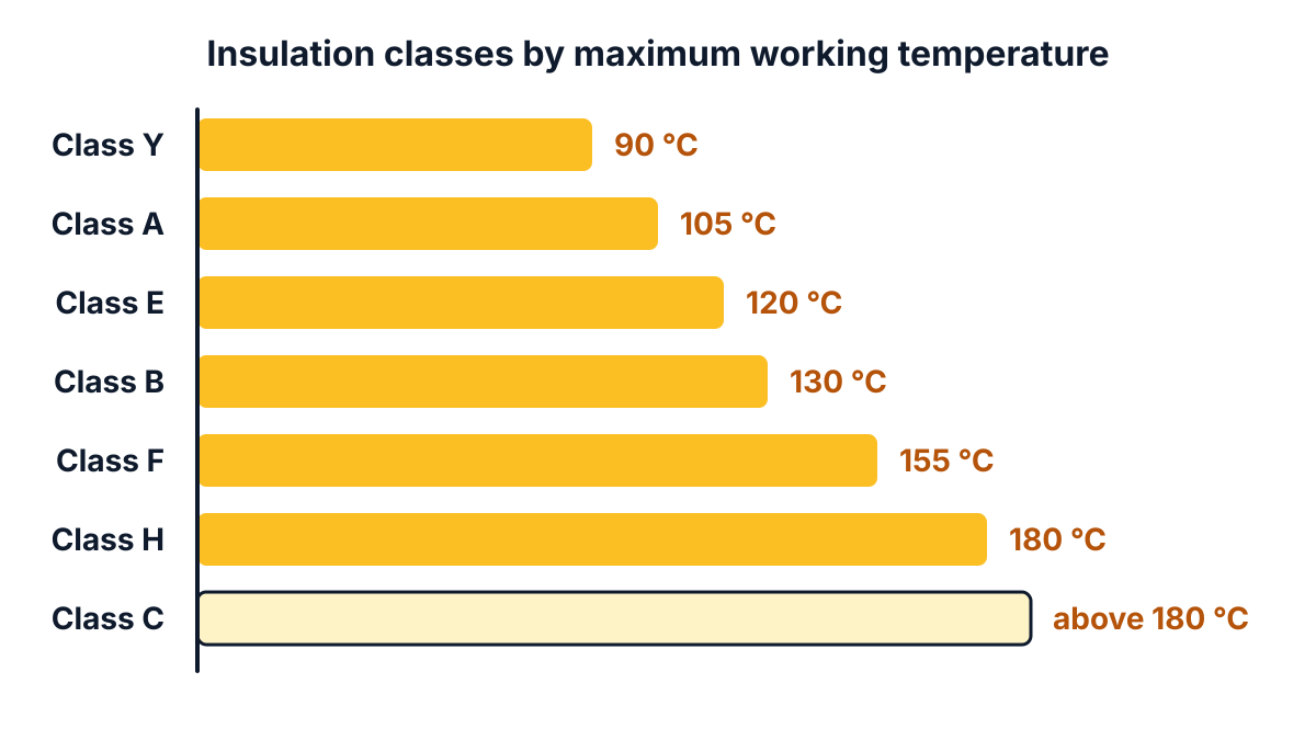
Figure Q3: thermal classes of insulation; each class can safely work up to the temperature shown.
Key points to write: classes Y, A, E, B, F, H, C with 90, 105, 120, 130, 155, 180 and above 180 °C, one example each.
Q4. What are the factors affecting Dielectric loss? (3 marks)
Understand it first
- A dielectric is an insulating material placed in an electric field, for example the insulation between capacitor plates.
- In a perfect dielectric under AC, the current leads the voltage by exactly 90°. Then no power is used up.
- A real dielectric is not perfect. Its current leads by a little less than 90°. The small missing angle is called the loss angle, δ (delta).
- Because of this, a little power is turned into heat inside the dielectric. This waste is the dielectric loss.
- The loss is given by P = 2πf C V² tan δ. Here f is frequency, C is capacitance, V is voltage and tan δ is the dissipation factor.
An analogy: bend a steel ruler back and forth fast. It gets warm. The molecules of a dielectric are also pushed back and forth by AC, and that “rubbing” makes heat.
Reading the formula tells you the factors. Loss rises with frequency (f), with voltage (V²), and with anything that raises tan δ, such as heat and moisture.
Exam answer (3 marks)
- Frequency: dielectric loss increases as the supply frequency increases (P ∝ f), because the molecules are pushed back and forth more times each second.
- Voltage and temperature: loss increases with the square of the applied voltage (P ∝ V²), and it increases as the temperature of the dielectric rises.
- Moisture (humidity): absorbed moisture greatly increases the loss angle δ and so the loss; dry, clean insulation has the lowest loss. Formula: P = 2πf C V² tan δ watts.
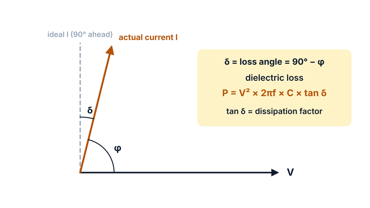
Figure Q4: in a real dielectric the current leads the voltage by φ, a little less than 90°; the loss angle δ = 90° − φ sets the dielectric loss.
Key points to write: frequency, voltage, temperature, moisture; P = 2πf C V² tan δ.
Q5. Classify the magnetic materials with examples. (3 marks)
Understand it first
- A magnetic material is one that reacts to a magnetic field in some way.
- Relative permeability, μᵣ, tells how easily a material lets magnetic flux pass compared with air. Air has μᵣ = 1.
- Every atom acts like a tiny magnet because of its moving electrons. How these tiny magnets behave decides the class.
There are three classes:
- Diamagnetic: pushes the field lines out a little. A magnet weakly repels it. μᵣ is slightly less than 1.
- Paramagnetic: pulls the field lines in a little, so it is weakly attracted. μᵣ is slightly more than 1.
- Ferromagnetic: field lines crowd into it very strongly. It is strongly attracted, and μᵣ is very large.
An analogy: a crowd walking down a road (the field). A diamagnetic block is like a puddle people walk around. A paramagnetic block is a shop a few people enter. A ferromagnetic block is a free-food stall that everyone crowds into.
Exam answer (3 marks)
- Diamagnetic materials: weakly repelled by a magnet; μᵣ slightly less than 1. Examples: copper, bismuth, silver, water.
- Paramagnetic materials: weakly attracted by a magnet; μᵣ slightly greater than 1. Examples: aluminium, platinum, manganese, oxygen.
- Ferromagnetic materials: strongly attracted by a magnet; μᵣ very large. Examples: iron, nickel, cobalt and their alloys.
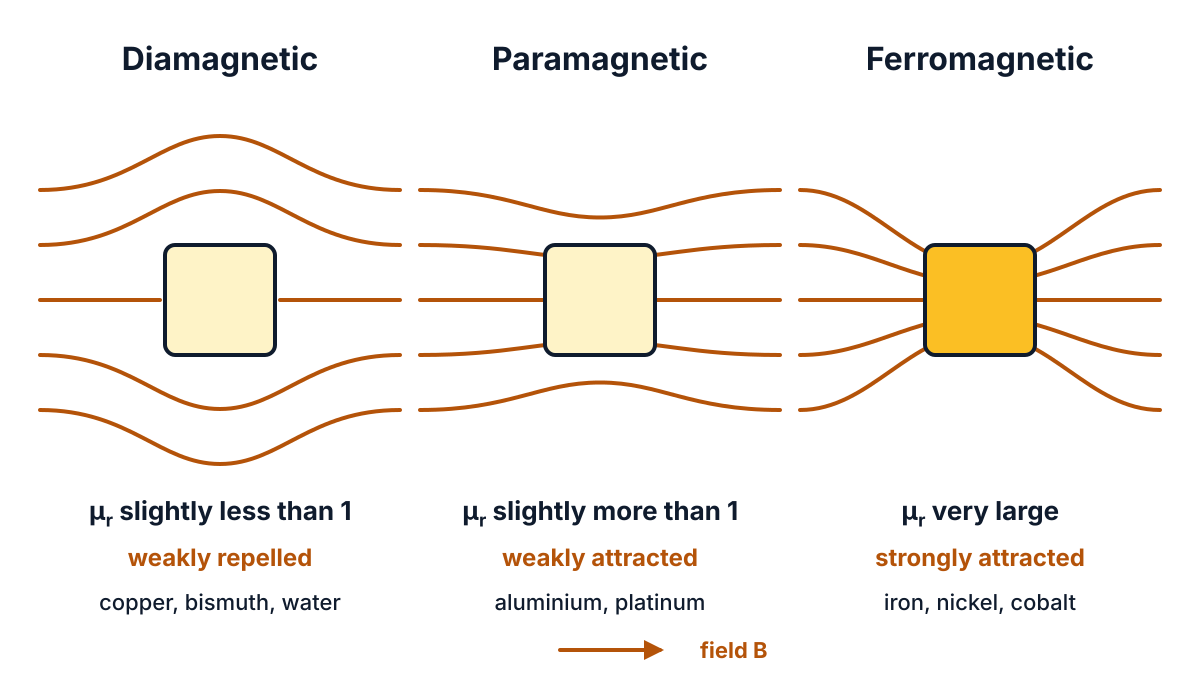
Figure Q5: a diamagnetic sample pushes field lines away, a paramagnetic sample draws a few in, and a ferromagnetic sample crowds them in.
Key points to write: dia (μᵣ < 1, copper), para (μᵣ slightly > 1, aluminium), ferro (μᵣ very large, iron).
Q6. Define co-efficient of coupling of two coils. (3 marks)
Understand it first
- When current flows in a coil, it makes magnetic flux (φ), the magnetic lines passing through the coil.
- Place a second coil near the first. Some of the first coil’s flux also passes through the second coil. This shared flux is the mutual flux.
- The rest of the flux misses the second coil. It is called leakage flux.
- Mutual inductance (M) measures how well one coil’s changing current induces an emf in the other. Self-inductance (L) measures the same thing for a coil acting on itself.
- The coefficient of coupling (k) tells what fraction of the flux of one coil links the other.
An analogy: two people standing under one umbrella in the rain. If they stand close, both stay dry (all the umbrella’s cover is shared). If they stand apart, one gets wet. Close coils on one iron core share almost all their flux. Coils far apart in air share very little.
Example: L₁ = 4 mH, L₂ = 9 mH and M = 3 mH. Then √(L₁L₂) = √36 = 6 mH, and k = 3 / 6 = 0.5. So half the flux is shared.
Exam answer (3 marks)
- Definition: the coefficient of coupling (k) of two coils is the fraction of the magnetic flux produced by one coil that links the other coil: k = φ₁₂ / φ₁.
- Formula: k = M / √(L₁L₂), where M is the mutual inductance and L₁, L₂ are the self-inductances of the two coils.
- Range: k lies between 0 and 1. When k = 1 the coils are tightly coupled (all flux links both, as on a common iron core); when k is near 0 they are loosely coupled.
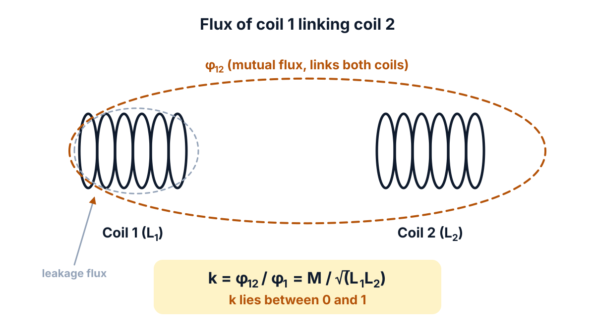
Figure Q6: only the mutual flux φ₁₂ links both coils; the leakage flux links coil 1 alone, so k = φ₁₂ / φ₁ is less than 1.
Key points to write: fraction of flux linking the other coil; k = M / √(L₁L₂); 0 ≤ k ≤ 1.
Q7. State Fleming’s left hand rule. (3 marks)
Understand it first
- A wire carrying current makes its own magnetic field around it.
- Put that wire between the poles of a magnet. The two fields push on each other.
- The result is a mechanical force on the wire. The wire moves. This is how every electric motor turns.
- The force, the field and the current are always at right angles to each other.
- Fleming’s left hand rule is a quick way to find the direction of that force.
How to use your hand:
- Hold your left hand out.
- Stretch the thumb, forefinger and middle finger so that each is at 90° to the other two.
- Point the forefinger along the field (north to south).
- Point the middle finger along the current.
- The thumb now shows the thrust, that is, the force or motion.
Memory aid: “FBI”. Thumb = F (force), forefinger = B (field), middle finger = I (current).
Remember: the left hand is for motors. The right hand rule is for generators.
Exam answer (3 marks)
- Statement: stretch the thumb, forefinger and middle finger of the left hand so that they are mutually perpendicular to each other.
- Fingers: if the forefinger points in the direction of the magnetic field and the middle finger in the direction of the current, then the thumb points in the direction of the force (motion) on the conductor.
- Use: the rule gives the direction of rotation of electric motors; the magnitude of the force is F = BIl sin θ newtons.
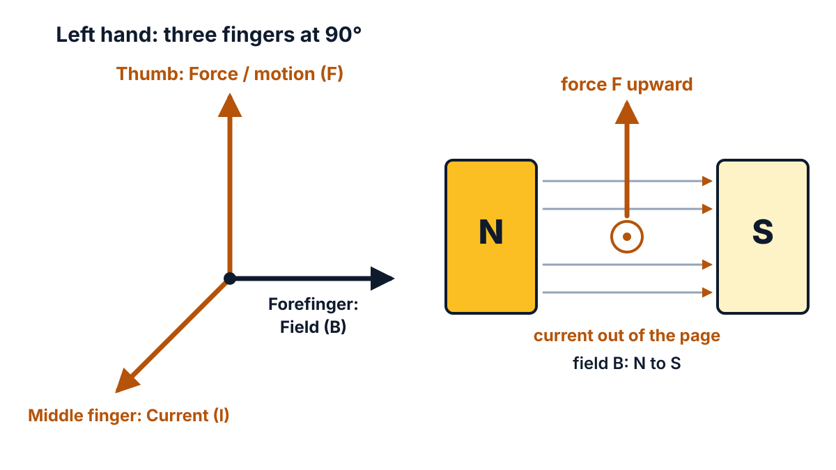
Figure Q7: forefinger = field, middle finger = current, thumb = force; with the field from N to S and current out of the page, the conductor is pushed upward.
Key points to write: left hand, three fingers at 90°; forefinger field, middle finger current, thumb force; used for motors.
Q8. State Faraday’s laws of electromagnetic induction. (3 marks)
Understand it first
- Magnetic flux (φ) is the amount of magnetic lines passing through a coil. It is measured in webers (Wb).
- Flux linkage is the flux multiplied by the number of turns, Nφ.
- Electromagnetic induction means producing an emf (a voltage) in a coil by changing the flux through it.
- The key word is change. A magnet sitting still inside a coil gives nothing. Move it in or out, and a voltage appears.
Faraday found two facts:
- A change of flux produces an emf. That is the first law.
- The faster the change, the bigger the emf. That is the second law.
An analogy: a turnstile counts people. A crowd standing still does not turn it. Only people passing through do. And the more people pass per second, the faster it turns.
The minus sign in e = −N dφ/dt comes from Lenz’s law. It says the induced emf always opposes the change that causes it.
Exam answer (3 marks)
- First law: whenever the magnetic flux linked with a coil (or conductor) changes, an emf is induced in it. If the circuit is closed, an induced current flows.
- Second law: the magnitude of the induced emf is equal to the rate of change of flux linkages.
- Formula: e = N dφ/dt volts (with Lenz’s law, e = −N dφ/dt), where N is the number of turns and dφ/dt is the rate of change of flux in Wb/s.
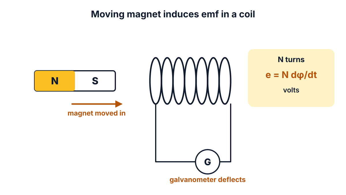
Figure Q8: moving the magnet changes the flux through the coil, so an emf e = N dφ/dt is induced and the galvanometer deflects.
Key points to write: change of flux induces emf; emf equals rate of change of flux linkages; e = N dφ/dt.
Q9. State Gauss theorem. (3 marks)
Understand it first
- An electric charge (Q) spreads an electric field around it. We show the field with lines, called lines of electric flux.
- Electric flux (ψ, psi) is the total number of these lines. In SI units, a charge of Q coulombs sends out a flux of Q coulombs.
- A closed surface is a surface with no opening, like a balloon or a box with its lid on. It has an inside and an outside.
- Gauss theorem links the flux leaving a closed surface to the charge inside it.
Think of a sprinkler inside a tent. All the water it throws must come out through the tent walls, whatever the tent’s shape. Count the water leaving, and you know how strong the sprinkler is. A sprinkler outside the tent sends water in on one side and out on the other, so it adds nothing in total.
The shape of the surface and the charges outside it do not matter.
Exam answer (3 marks)
- Statement: the total electric flux passing out through any closed surface is equal to the total charge enclosed by that surface.
- Formula: ψ = ΣQ (flux in coulombs); in terms of field intensity in air, the total flux of E through the surface = ΣQ / ε₀.
- Note: charges outside the surface contribute nothing to the net flux, and the shape of the surface does not matter. The theorem is used to find the field of charged spheres, wires and plates.
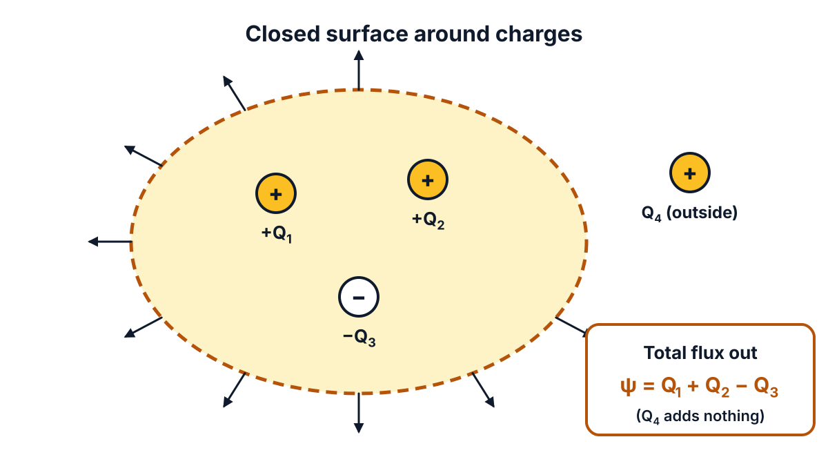
Figure Q9: the flux leaving the closed surface equals the charge inside, Q₁ + Q₂ − Q₃; the outside charge Q₄ adds nothing.
Key points to write: total flux out of a closed surface = total charge enclosed; ψ = ΣQ.
Q10. Define Electric field density. (3 marks)
Understand it first
The paper prints “Electric field density”, which is not a standard term; the C-23 syllabus has electric flux density and electric field intensity, so the question most likely means electric flux density, answered below.
- Electric flux (ψ) is the total amount of electric lines coming from a charge. It is measured in coulombs (C).
- Density means “how much per unit area”. Like population density is people per square kilometre.
- Electric flux density (D) is the flux passing through one square metre of area, held at right angles to the flux.
- Electric field intensity (E) is the force on a charge of one coulomb placed at a point, in newtons per coulomb (N/C) or volts per metre.
- The two are linked by the material: D = ε₀εᵣE. Here ε₀ is the permittivity of free space and εᵣ is the relative permittivity of the material.
An analogy: rain falling on a courtyard. Total rain is the flux. Rain per square metre is the flux density. Hold a bucket flat (at right angles to the rain) to catch the most.
Exam answer (3 marks)
- Definition: electric flux density (D) at a point is the electric flux passing normally through unit area at that point.
- Formula and unit: D = ψ / A, where ψ is the flux in coulombs and A is the area in m² held normal to the flux. Unit: coulomb per square metre (C/m²).
- Relation: D = ε₀εᵣE, where E is the electric field intensity in V/m; for a point charge Q at distance r, D = Q / (4πr²).
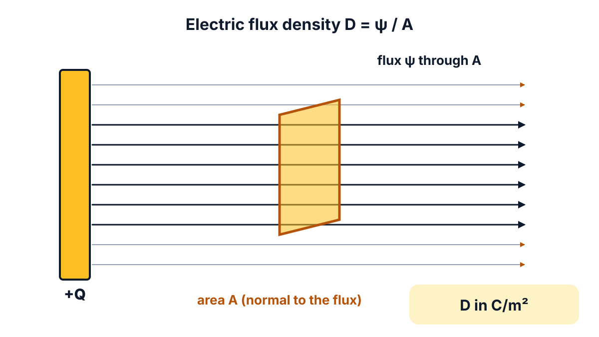
Figure Q10: the flux ψ crossing an area A held normal to it gives the flux density D = ψ / A, in C/m².
Key points to write: flux per unit normal area; D = ψ / A in C/m²; D = ε₀εᵣE.
Q11. Mention the properties and applications of Manganin and Constantan. (10 marks)
Understand it first
- Most metals change their resistance when they get hot. Copper’s resistance rises a lot with temperature.
- The temperature coefficient of resistance tells how much resistance changes for each degree of temperature change. A small value means the resistance hardly changes.
- Some jobs need a resistance that stays fixed, whatever the temperature. Examples: standard resistors in a laboratory, and shunts in ammeters. A shunt is a low resistance connected across a meter to carry most of the current.
- For such jobs we use alloys. An alloy is a mixture of metals. The two most common ones are Manganin and Constantan.
- Both are high resistivity materials: for the same size, they oppose current much more than copper.
What is in them:
- Manganin is copper with some manganese and a little nickel. A maker’s data sheet for Manganin gives about 12% manganese, 2% nickel and the rest (86%) copper.
- Constantan is copper with a lot of nickel. A maker’s data sheet for constantan gives about 44% nickel, 1% manganese and the rest (55%) copper.
Books give slightly different percentages, because each maker uses a slightly different mix. Any standard figure is accepted in the exam.
Why do we need two alloys? The key difference is the thermal emf against copper. Where two different metals touch and are warm, a tiny voltage appears. Manganin gives almost none against copper (about 1 µV per °C). Constantan gives a lot (about 40 µV per °C). So Manganin is best for precise measuring resistors, and Constantan is used where that voltage is welcome, as in thermocouples (temperature sensors), or where it does not matter, as in heaters and rheostats.
An analogy: a good wooden ruler keeps its length in summer and winter. Manganin and Constantan are the “good rulers” of resistance.
Exam answer (10 marks)
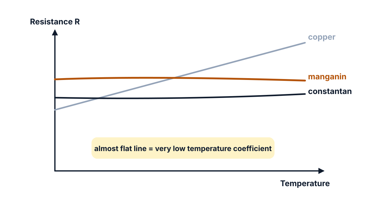
Figure Q11: the resistance of copper rises steeply with temperature, but the curves of Manganin and Constantan are almost flat.
The split assumed is 5 marks for Manganin and 5 marks for Constantan.
(a) Manganin (5 marks)
- Composition: an alloy of copper, manganese and nickel, about 86% Cu, 12% Mn and 2% Ni.
- High resistivity and very low temperature coefficient: resistivity about 0.43 µΩ m, and its resistance hardly changes between room temperature and about 50 °C.
- Very low thermal emf against copper and high stability: its resistance stays the same over many years, so readings do not drift.
- Applications (precision): standard resistances, resistance boxes and precision resistors in measuring instruments and bridges.
- Applications (meters): shunts of ammeters and series (multiplier) resistances of voltmeters.
(b) Constantan (5 marks)
- Composition: an alloy of copper and nickel, about 55% Cu, 44% Ni and 1% Mn.
- High resistivity and low temperature coefficient: resistivity about 0.49 µΩ m, almost constant over a wide range of temperature (hence the name “constantan”).
- Other properties: good resistance to oxidation and corrosion, non-magnetic, easily drawn into thin wire and soldered, and usable up to a higher temperature than Manganin; but it has a high thermal emf against copper.
- Applications (resistors): wire-wound resistors, rheostats, potentiometers and starter or regulator resistances.
- Applications (heat): low-temperature heating elements and heating cables, and thermocouples (with copper or iron) and their compensating cables, because of its high thermal emf.
Conclusion: Manganin is preferred for precision and standard resistors; Constantan is preferred for rheostats, heaters and thermocouples.
Q12. Explain the formation of N type semiconductors with a neat sketch of diagram. (10 marks)
Question (as printed): 12. Explain the formation of N type semiconductors with a neat sketch of diagram. 10
Understand it first
- Silicon (Si) and germanium (Ge) are the basic semiconductors. Each atom has 4 valence electrons (outer-shell electrons). Such an atom is called tetravalent.
- In a crystal, each silicon atom shares one electron with each of its 4 neighbours. A shared pair of electrons is a covalent bond.
- In pure silicon, all 4 valence electrons are busy in bonds. Very few are free to move. So pure silicon (an intrinsic semiconductor) conducts poorly at room temperature.
- Doping is adding a very small, controlled amount of another element (an impurity) to the pure crystal. The doped crystal is an extrinsic semiconductor.
- A pentavalent atom has 5 valence electrons. Examples: phosphorus (P), arsenic (As) and antimony (Sb).
What happens when an arsenic atom takes the place of a silicon atom:
- Arsenic has 5 valence electrons.
- Four of them make covalent bonds with the 4 silicon neighbours, exactly as a silicon atom would.
- The fifth electron has no bond to join. It is held only weakly by the arsenic atom.
- Even the heat of a normal room is enough to set it free. It can now wander through the crystal and carry current.
- Every arsenic atom gives one free electron. So the impurity is called a donor.
Now the crystal has many free electrons. Electrons carry negative charge, so the material is called N-type (N for negative).
An analogy: a classroom where students sit in pairs at desks of two. Add a group of five friends to a desk row built for four. Four sit down. The fifth has no seat and walks around freely. That walking student is the free electron.
Two more facts often asked:
- A few holes (empty places in bonds) still form because heat breaks some bonds. In N-type material they are the minority carriers. Free electrons are the majority carriers.
- When the donor atom loses its fifth electron, it becomes a positive ion. This ion is fixed in the crystal and cannot move. The crystal as a whole stays electrically neutral, because the number of protons and electrons is still equal.
In energy terms, the donor electron sits in a donor level, very close below the conduction band (the band where electrons are free). A tiny bit of energy lifts it into the conduction band. The same idea for a single donor atom was asked as a short note in the EE-103 Physics paper of March 2026.
Exam answer (10 marks)
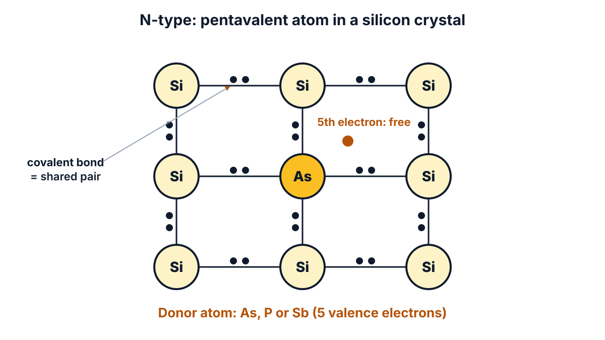
Figure Q12 (a): an arsenic atom in a silicon crystal; four electrons form covalent bonds and the fifth becomes a free electron.
- Definition: an N-type semiconductor is an extrinsic semiconductor formed by adding a small amount of pentavalent impurity to a pure semiconductor such as silicon or germanium.
- Pure crystal: silicon is tetravalent; each atom forms four covalent bonds with its four neighbours, so almost no free electrons are available.
- Impurity: a pentavalent impurity such as phosphorus, arsenic or antimony (5 valence electrons) is added in a very small quantity.
- Bond formation: the impurity atom replaces a silicon atom; four of its valence electrons form covalent bonds with the four neighbouring silicon atoms.
- Free electron: the fifth valence electron is not part of any bond. It is loosely bound and becomes free even at room temperature.
- Donor: each impurity atom donates one free electron to the crystal, so it is called a donor impurity.
- Donor ion: after giving away its electron, the impurity atom becomes a fixed (immobile) positive ion; the crystal remains electrically neutral.
- Carriers: free electrons are the majority carriers; holes produced by thermal breaking of bonds are the minority carriers.
- Energy level: the donor electrons occupy a donor energy level just below the conduction band, so they easily move into the conduction band.
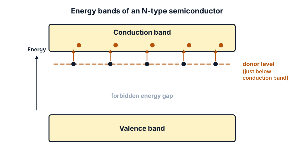
Figure Q12 (b): the donor level lies just below the conduction band, so donor electrons need very little energy to become free.
- Conduction: when a voltage is applied, the current is carried mainly by the free electrons, which move towards the positive terminal.
Conclusion: adding a pentavalent (donor) impurity to silicon or germanium gives an N-type semiconductor, in which electrons are the majority carriers.
Q13. Mention the properties and applications of Impregnated paper and PVC. (10 marks)
Understand it first
- Plain paper is made of cellulose fibres. It is cheap and a good insulator when dry.
- But plain paper soaks up moisture from the air. A material that absorbs moisture is called hygroscopic. Wet paper is a poor insulator.
- Impregnated means soaked through. Paper is dried and then soaked in insulating oil, varnish, wax or resin. The oil fills the tiny air gaps and keeps moisture out.
- This raises its dielectric strength: the highest voltage the material can stand without breaking down.
- PVC means polyvinyl chloride. It is a thermoplastic: a plastic that softens on heating and hardens again on cooling, so it can be moulded many times.
- PVC is made from vinyl chloride by addition polymerisation, as explained in the EE-104 Chemistry paper of March 2026.
Pure PVC is hard and stiff. Makers mix in other substances (the C-23 syllabus asks about these):
- Plasticizer: makes PVC soft and flexible, so cable insulation can bend.
- Stabilizer: protects PVC from breaking down under heat and light.
- Filler: cheap powder (such as chalk) that lowers cost and adds bulk and strength.
- Additives: colours, flame retardants and similar extras.
An analogy: a dry sponge soaks up water. Fill the sponge with oil first, and water cannot get in. That is impregnation.
Exam answer (10 marks)
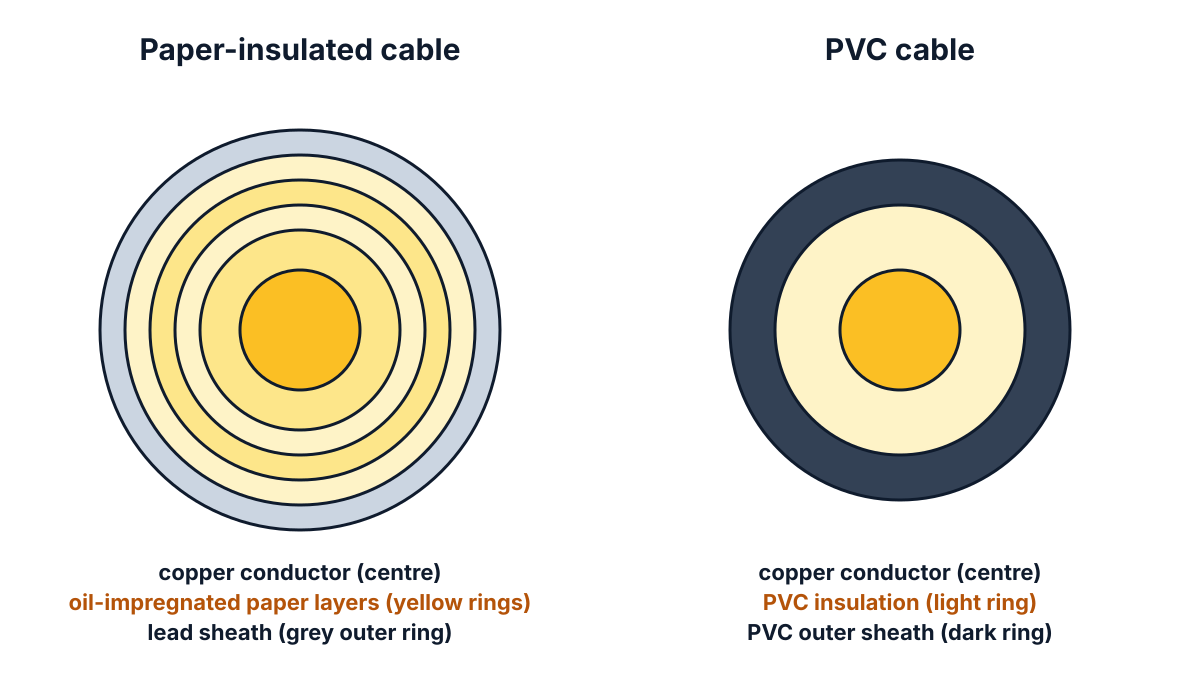
Figure Q13: a paper-insulated cable uses layers of oil-impregnated paper under a lead sheath; a PVC cable uses PVC for both insulation and outer sheath.
The split assumed is 5 marks for impregnated paper and 5 marks for PVC.
(a) Impregnated paper (5 marks)
- Meaning: paper (cellulose) that is dried and then impregnated with insulating oil, varnish, wax or resin to remove moisture and fill the air spaces.
- Electrical properties: high dielectric strength and high insulation resistance; impregnation also reduces dielectric loss.
- Other properties: cheap, light and flexible, easy to wind in layers; impregnation makes it non-hygroscopic. It belongs to class A insulation (105 °C).
- Applications (cables): insulation of high voltage underground power cables (paper-insulated, lead-sheathed cables).
- Applications (machines): insulation in capacitors (paper capacitors), and between layers of transformer windings and coils.
(b) PVC, polyvinyl chloride (5 marks)
- Meaning: a thermoplastic polymer of vinyl chloride, used with plasticizer, stabilizer and fillers.
- Electrical properties: good insulator with good dielectric strength and high insulation resistance at normal temperatures.
- Other properties: tough, flexible (with plasticizer), light, water-proof, resistant to oils, acids and alkalis, does not easily catch fire (self-extinguishing), cheap and easily coloured; it softens at higher temperatures, so it is used only for low-temperature work.
- Applications (wiring): insulation and outer sheath of house-wiring wires, flexible cords and low voltage power cables.
- Applications (other): conduit pipes and casing for wiring, insulating tapes and sleeves, and parts of switches, plugs and sockets.
Conclusion: impregnated paper is used where high voltage and steady conditions exist (cables, capacitors); PVC is used for everyday low voltage wiring.
Q14. Explain polarization of Dielectric material with a neat sketch of diagram. (10 marks)
Understand it first
- A dielectric is an insulating material, like mica, glass, paper or oil. It has no free electrons, so no current flows through it.
- But its charges can still shift a little. Every atom has a positive centre (the nucleus) and a cloud of negative electrons around it.
- With no electric field, the centre of the electron cloud sits exactly on the nucleus. The positive and negative charges balance at one point.
- Apply an electric field (E). The field pushes the nucleus a little along E and pulls the electron cloud a little the other way.
- Now the positive and negative centres are separated by a small distance d. A pair of equal and opposite charges separated by a distance is an electric dipole.
- The strength of a dipole is its dipole moment: p = q × d.
- Polarization is this formation and lining up of dipoles inside a dielectric when a field is applied.
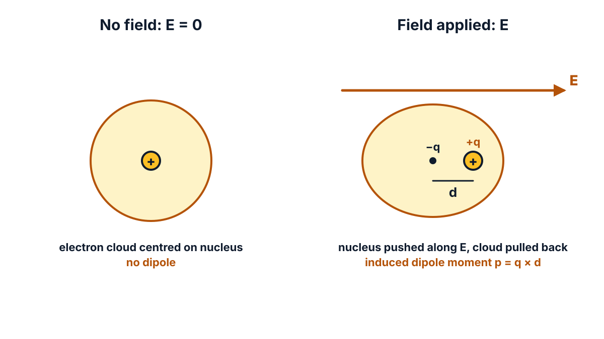
Figure Q14 (a): with no field the electron cloud is centred on the nucleus; in a field E the centres separate by d and the atom becomes a dipole, p = q × d.
What happens in a whole slab between two capacitor plates:
- Every atom becomes a small dipole, all pointing the same way.
- Inside the slab, the + end of one dipole sits next to the − end of the next. They cancel.
- At the surfaces they do not cancel. A layer of negative charge appears on the face next to the positive plate. A layer of positive charge appears on the face next to the negative plate. These are bound charges: they cannot leave the material.
- The bound charges make a field opposite to the applied field. So the net field inside the dielectric becomes smaller.
- For the same voltage, the plates can now hold more charge. That is why a dielectric increases capacitance by εᵣ times.
An analogy: a class of students sitting in random directions. The teacher calls “face the board” and everyone turns the same way. The field is the teacher’s call; the students turning is polarization.
Exam answer (10 marks)
- Definition: polarization is the displacement of the positive and negative charges in a dielectric under an applied electric field, so that each atom or molecule becomes an electric dipole aligned with the field.
- Without field: in each atom the centre of the negative electron cloud coincides with the positive nucleus, so there is no dipole moment.
- With field: the nucleus is pushed along the field and the electron cloud is pulled opposite to it; their centres separate by a small distance d.
- Dipole moment: each displaced atom forms an induced dipole of moment p = q × d (coulomb metre).
- Polarization vector: the dipole moment per unit volume of the dielectric is called the polarization P; its unit is C/m².
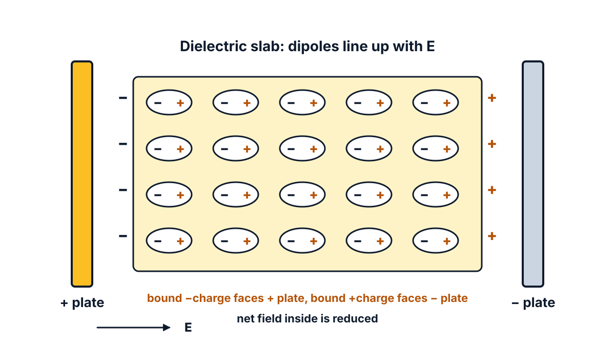
Figure Q14 (b): the dipoles line up with E; bound negative charge faces the positive plate and bound positive charge faces the negative plate.
- Bound charges: inside the slab neighbouring dipoles cancel, but negative bound charge appears on the surface facing the positive plate and positive bound charge on the surface facing the negative plate.
- Effect on field and capacitance: the bound charges set up a field opposite to the applied field, so the net field in the dielectric falls and the capacitance rises by the factor εᵣ.
- Electronic polarization: displacement of the electron cloud relative to the nucleus; it occurs in all dielectrics (for example, mica, glass).
- Ionic polarization: in ionic materials such as sodium chloride, positive ions shift along the field and negative ions opposite to it.
- Orientation polarization: in materials with permanent dipoles (such as water and some oils), the randomly pointing dipoles turn to line up with the field; this type depends strongly on temperature.
Conclusion: polarization creates bound surface charges that reduce the field inside a dielectric and increase the capacitance; it is also the source of dielectric loss under AC.
Q15. Explain different types of Magnetic materials. (10 marks)
Understand it first
- Every electron spins and moves round its nucleus. Each such motion makes a tiny magnet. The strength of this tiny magnet is its magnetic moment.
- In many atoms these tiny magnets cancel in pairs. In some atoms they do not cancel, and the atom itself is a small magnet.
- Relative permeability (μᵣ) compares how easily flux passes through the material with how easily it passes through air (μᵣ = 1).
- Magnetic susceptibility tells how strongly the material is magnetised by a field. It is negative for diamagnetic materials and positive for the others.
The three types, in simple words:
- Diamagnetic: the atoms have no net magnetic moment of their own. An outside field makes a small opposing moment, so the material is weakly repelled.
- Paramagnetic: each atom is a tiny magnet, but they point in random directions. A field lines up a few of them, so the material is weakly attracted. Heat shakes them out of line again.
- Ferromagnetic: the tiny atomic magnets line up with each other in small regions called domains. A field makes the domains grow and turn, so the material becomes a strong magnet.
An analogy for ferromagnetism: a school assembly. Each class (domain) already faces one way, but different classes face different ways. When the principal speaks from the stage (the field), whole classes turn together. That is why the effect is so strong.
Two more ideas from the C-23 syllabus:
- Curie point: above a certain temperature, called the Curie temperature, a ferromagnetic material loses its domains and becomes paramagnetic.
- Soft and hard magnetic materials: soft ones (silicon steel, soft iron) magnetise and demagnetise easily, with a narrow hysteresis loop; they are used for transformer and motor cores. Hard ones (alnico, cobalt steel) keep their magnetism; they are used for permanent magnets.
Exam answer (10 marks)
Magnetic materials are classified, by their behaviour in a magnetic field, into diamagnetic, paramagnetic and ferromagnetic materials.
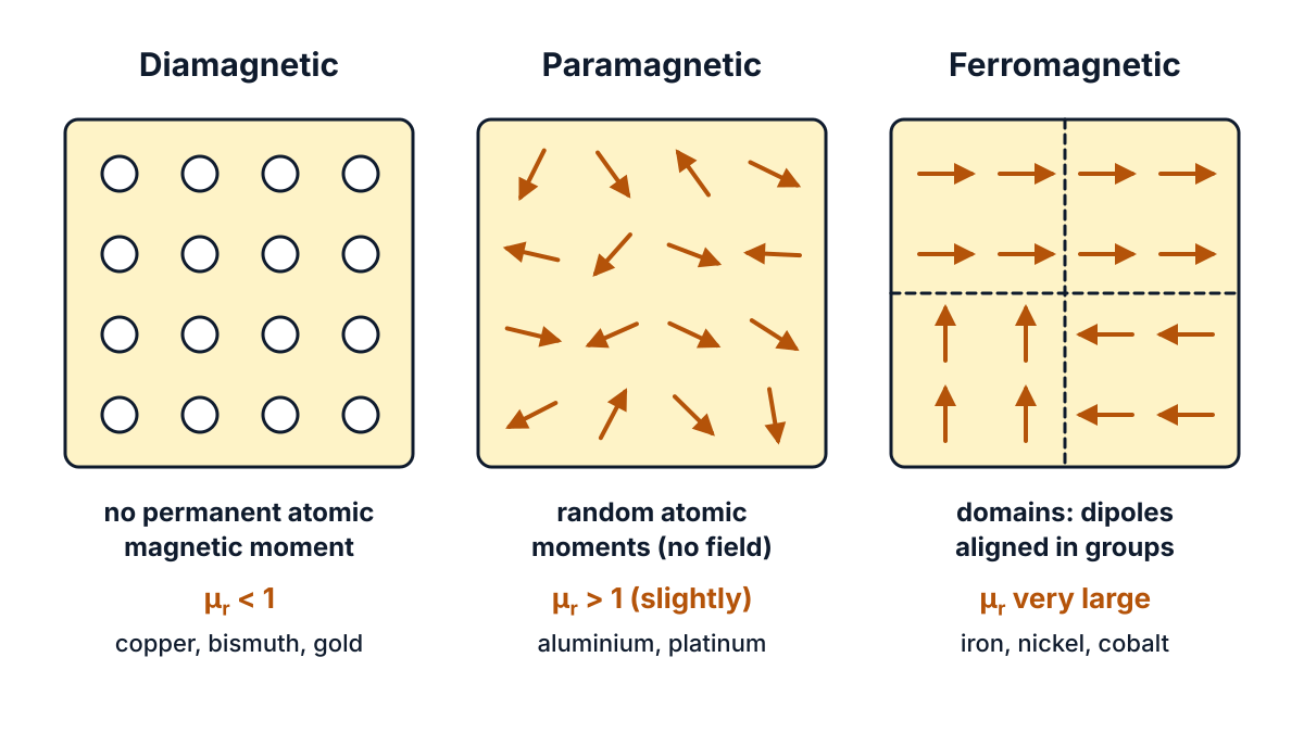
Figure Q15: diamagnetic atoms have no permanent moment, paramagnetic moments point at random, and ferromagnetic moments are aligned inside domains.
Diamagnetic materials
- Nature: the atoms have no permanent magnetic moment; an applied field induces a weak moment opposite to the field, so the material is weakly repelled by a magnet.
- Permeability: μᵣ is slightly less than 1 and the susceptibility is small and negative, almost independent of temperature.
- Examples: copper, silver, gold, bismuth, zinc, water.
Paramagnetic materials
- Nature: each atom has a small permanent magnetic moment, but the moments point in random directions; a field aligns them slightly, so the material is weakly attracted.
- Permeability: μᵣ is slightly greater than 1 and the susceptibility is small and positive; it decreases as the temperature rises.
- Examples: aluminium, platinum, manganese, chromium, oxygen.
Ferromagnetic materials
- Nature: the atomic moments are aligned in groups called domains; a field makes the domains grow and turn into line, so the material is strongly attracted and strongly magnetised.
- Permeability: μᵣ is very large (hundreds to thousands) and not constant; it changes with the field, giving a B-H curve with saturation and hysteresis.
- Curie point: above the Curie temperature a ferromagnetic material loses its ferromagnetism and behaves as a paramagnetic material.
- Examples and uses: iron, nickel, cobalt and their alloys; soft ferromagnetic materials (silicon steel) for transformer and machine cores, hard ones (alnico) for permanent magnets.
Conclusion: only ferromagnetic materials are useful as magnetic cores and magnets; dia- and paramagnetic materials are treated as non-magnetic in electrical engineering.
Q16. Derive expression for magnitude of the force on a current carrying conductor in a magnetic field. (10 marks)
Question (as printed): 16. Derive expression for magnitude of the force on a current carrying conductor in a magnetic field. 10
Understand it first
- Magnetic flux density (B) tells how strong a magnetic field is. It is the flux per square metre, measured in tesla (T) or Wb/m².
- A current-carrying wire has its own circular field around it. When it lies in another field, the two fields add on one side and cancel on the other.
- The field lines behave like stretched rubber bands. They push the wire from the crowded side towards the weak side. That push is the force (F) on the conductor.
- Experiments show that the force grows when you increase the field, the current or the length of wire inside the field.
- The angle also matters. A wire lying along the field lines feels no force at all. A wire at right angles to the field feels the biggest force.
Why the angle matters: split the field B into two parts.
- B cos θ runs along the wire. It is like pushing a pencil along its own length on a table. Nothing turns. No force.
- B sin θ runs at right angles to the wire. Only this part pushes the wire sideways.
Example: B = 0.5 T, I = 10 A, l = 0.2 m, θ = 30°. Then F = 0.5 × 10 × 0.2 × sin 30° = 0.5 × 10 × 0.2 × 0.5 = 0.5 N. At θ = 90° the same wire feels F = 0.5 × 10 × 0.2 = 1 N, and at θ = 0° it feels no force.
The idea of magnetic lines of force, which this derivation leans on, was asked in the EE-103 Physics paper of March 2025.
Exam answer (10 marks)
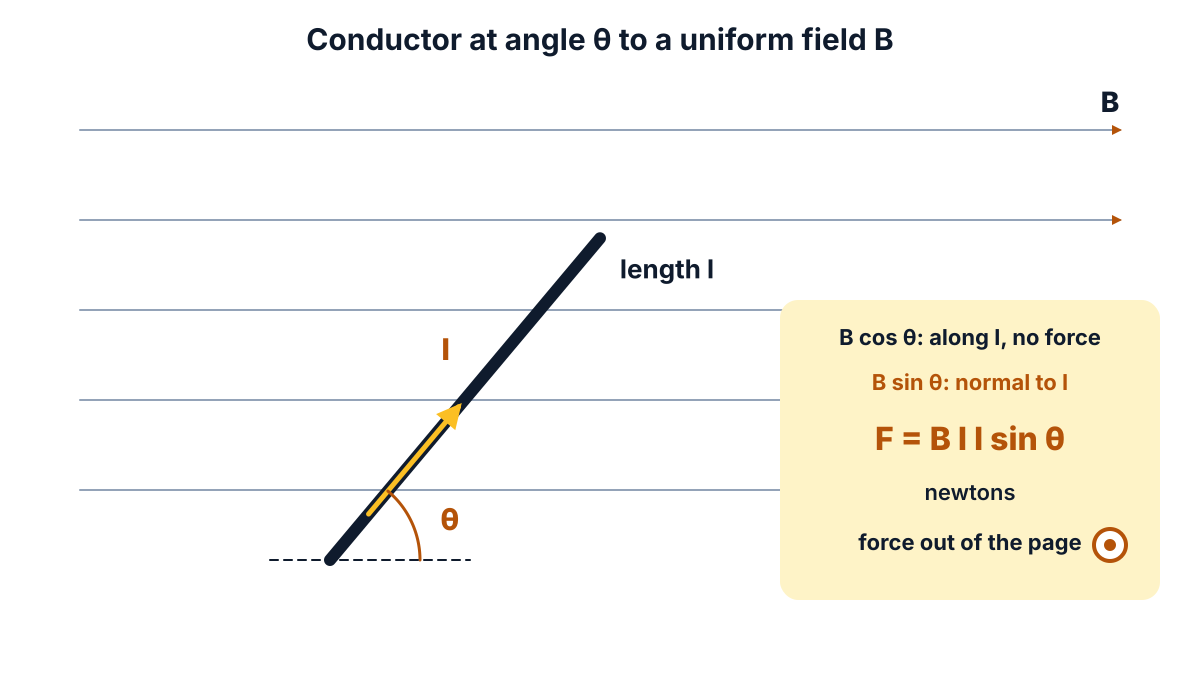
Figure Q16: only the component B sin θ, normal to the conductor, produces force; B cos θ along the conductor produces none.
- Set-up: consider a straight conductor of length l metres carrying a current I amperes, placed in a uniform magnetic field of flux density B Wb/m², making an angle θ with the direction of the field.
- Resolving B: resolve B into two components: B cos θ along the conductor and B sin θ perpendicular to the conductor.
- Component along the conductor: B cos θ is parallel to the current, so it produces no force on the conductor.
- Effective component: only B sin θ, perpendicular to the conductor, produces a force.
- Experimental facts: the force F is directly proportional to (i) the flux density, F ∝ B sin θ; (ii) the current, F ∝ I; and (iii) the length of conductor in the field, F ∝ l.
- Combining: F ∝ B I l sin θ, so F = k B I l sin θ, where k is a constant.
- Choice of units: in SI units k = 1, because unit flux density (1 Wb/m² or 1 tesla) is defined as the field in which a conductor 1 m long carrying 1 A at right angles to the field experiences a force of 1 N.
- Result: F = B I l sin θ newtons.
- Special cases: when θ = 90° (conductor at right angles to the field), F = B I l, the maximum value; when θ = 0° (conductor along the field), F = 0.
- Direction: the force acts at right angles to both the conductor and the field; its direction is given by Fleming’s left hand rule (Q7).
Answer: F = B I l sin θ newtons; maximum F = B I l when the conductor is perpendicular to the field.
Q17. Derive expression for energy stored in magnetic field. (10 marks)
Understand it first
- An inductor is a coil of wire. Its self-inductance (L), in henry (H), tells how strongly it opposes a change in its own current.
- When you switch on a coil, the current does not jump to its final value at once. It rises from zero to I over a short time.
- While the current rises, the flux of the coil rises too. A changing flux induces an emf (Faraday’s law, Q8).
- This self-induced emf is e = L di/dt. By Lenz’s law it opposes the rise of current. It is often called the back emf.
- The supply must push current against this back emf. Pushing against an opposing voltage means doing work. That work does not turn into heat; it is stored in the magnetic field of the coil.
- When the current is switched off, the field collapses and gives the energy back. That is the spark you see at a switch that breaks an inductive circuit.
An analogy: pushing a heavy flywheel up to speed. You work hard while it speeds up. Once it spins steadily, no more push is needed, but the energy is stored in the spinning wheel. Try to stop it, and it pushes back. Current in an inductor behaves the same way.
A check without calculus: if the current rises evenly from 0 to I in t seconds, the back emf is L I / t and the average current is I / 2. Energy = emf × average current × time = (L I / t) × (I / 2) × t = ½ L I².
Example: a coil of L = 2 H carrying I = 3 A stores W = ½ × 2 × 3² = 9 J.
Exam answer (10 marks)
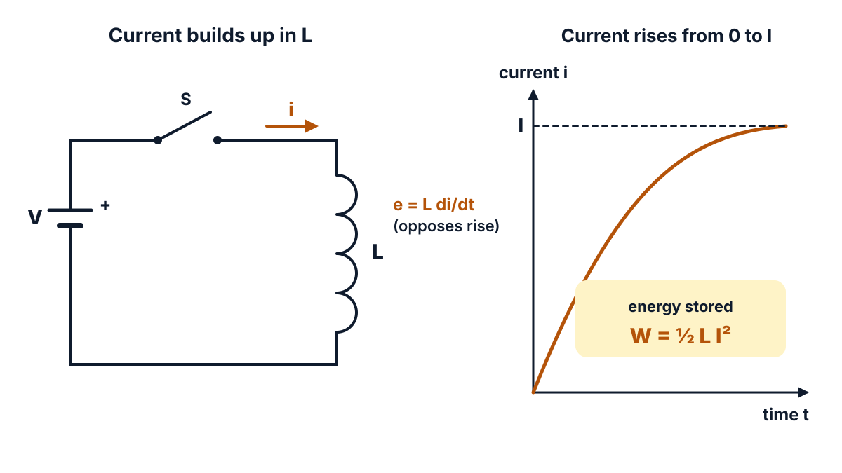
Figure Q17: when S is closed the current i rises from 0 to I against the back emf e = L di/dt, and the work done is stored as W = ½LI².
- Set-up: consider a coil of self-inductance L henry connected to a DC supply through a switch S. When S is closed, the current rises from zero to its final value I.
- Back emf: let i be the current at any instant, rising at the rate di/dt. A self-induced emf e = L di/dt is set up which opposes the rise of current (Lenz’s law).
- Power: to keep the current rising, the supply must supply power against this emf: p = e × i = L i (di/dt) watts.
- Energy in a small time: in a small time dt, the energy supplied is dW = p dt = L i (di/dt) dt = L i di.
- Total energy: the total energy supplied while the current rises from 0 to I is W = ∫₀ᴵ L i di.
- Integration: W = L [i² / 2] from 0 to I = ½ L I².
- Result: W = ½ L I² joules. This energy is stored in the magnetic field of the coil, not lost as heat.
- Return of energy: when the current falls to zero, the field collapses and the stored energy is returned to the circuit (seen as a spark at the switch).
- Energy per unit volume: for a long solenoid of length l, area A and N turns, L = μN²A / l and B = μNI / l, so W = (B² / 2μ) × A l; the energy stored per unit volume is B² / 2μ J/m³.
- Example: a coil of 2 H carrying 3 A stores W = ½ × 2 × 3² = 9 J.
Answer: energy stored in the magnetic field of an inductor, W = ½ L I² joules (B² / 2μ J/m³ per unit volume).
Q18. Obtain formula for capacitance of a parallel plate capacitor. (10 marks)
Understand it first
- A capacitor stores electric charge. The simplest one is two flat metal plates facing each other, with an insulator (a dielectric) between them.
- Connect it to a battery. One plate gets charge +Q and the other −Q. A voltage V appears between the plates.
- Capacitance (C) is the charge stored per volt: C = Q / V. Its unit is the farad (F).
- Permittivity (ε) tells how easily a material allows electric flux. ε₀ is the permittivity of free space (vacuum), 8.854 × 10⁻¹² F/m from the CODATA value. Relative permittivity (εᵣ) says how many times better a material is than vacuum.
How the formula is built, in plain words:
- The charge Q spreads evenly over the plate area A. So the flux density is D = Q / A.
- The field between the plates is E = D / (ε₀εᵣ).
- The field is uniform, so the voltage is just field × gap: V = E × d.
- Divide Q by V, and the charge cancels out. You get C = ε₀εᵣA / d.
So capacitance depends only on the shape and the material, not on the charge. Bigger plates hold more (like a bigger bucket). A smaller gap holds more (the plates pull the charges more strongly). A better dielectric holds more.
Example: plates of 0.01 m² with a gap of 1 mm (0.001 m) in air give C = 8.854 × 10⁻¹² × 0.01 / 0.001 = 8.854 × 10⁻¹¹ F = 88.54 pF. Put a dielectric of εᵣ = 5 in the gap, and C becomes 5 × 88.54 = 442.7 pF.
Exam answer (10 marks)
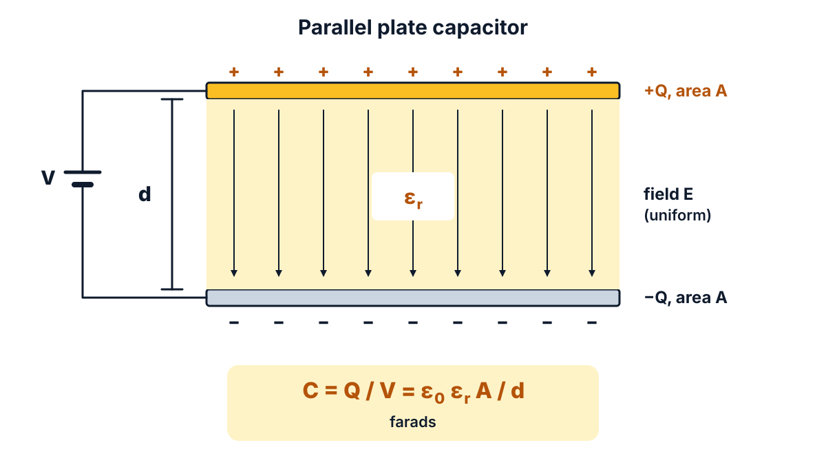
Figure Q18: plates of area A and separation d with a dielectric εᵣ; the uniform field E between them gives C = ε₀εᵣA / d.
- Set-up: consider two parallel metal plates, each of area A m², separated by a distance d metres, with a dielectric of relative permittivity εᵣ between them.
- Charge and voltage: let a potential difference V volts give charges +Q and −Q coulombs on the plates.
- Assumption: the field between the plates is uniform and fringing at the edges is neglected (d is small compared with the plate size).
- Flux density: the flux Q passes normally through area A, so D = Q / A C/m².
- Field intensity: E = D / (ε₀εᵣ) = Q / (ε₀εᵣA) V/m.
- Potential difference: for a uniform field, V = E × d = Q d / (ε₀εᵣA) volts.
- Capacitance: C = Q / V = Q ÷ [Q d / (ε₀εᵣA)].
- Result: C = ε₀εᵣA / d farads, where ε₀ = 8.854 × 10⁻¹² F/m.
- Air capacitor: with air or vacuum between the plates (εᵣ = 1), C₀ = ε₀A / d; so C / C₀ = εᵣ, and a dielectric increases the capacitance εᵣ times.
- Factors affecting capacitance: C is directly proportional to the plate area A and to the permittivity of the dielectric, and inversely proportional to the distance d between the plates.
Answer: C = ε₀εᵣA / d farads.
FAQ
Which units carry the most marks in the EE-105 October 2024 paper?
Unit 4 (magnetic effects of electric current and electromagnetic induction) carries 29 marks: Q6, Q7, Q8, Q16 and Q17. Units 1 and 2 carry 26 marks each. Unit 5 carries 16 and Unit 3 carries 13. These totals include the Part B choice, so they add up to 110, exactly the unit weightage of the C-23 syllabus.
Which five Part B questions should I choose in this paper?
Q18, Q16, Q17, Q12 and Q14 are the safest five. Each has a fixed set of steps and a standard figure, so the examiner can tick each point. Q11 and Q13 are good only if you have learnt the property lists of the four materials by heart.
Is ‘Electric field density’ in Q10 a misprint?
Yes, most likely. The C-23 syllabus has electric flux density and electric field intensity, but no ‘field density’. Answer electric flux density: D = ψ / A, in coulombs per square metre, and add one line that D = ε₀εᵣE links it to field intensity.
Do I have to write exact percentages for Manganin and Constantan in Q11?
Write the main metals and an approximate mix. A maker’s data sheet gives Manganin as copper with about 12% manganese and 2% nickel, and Constantan as copper with about 44% nickel. Books differ by a few percent between makers, and examiners accept any standard figure.
Sources
- AP SBTET C-23 DEEE EE-105 question paper, Oct-Nov 2024
- C-23 Curriculum, Diploma in Electrical and Electronics Engineering, SBTET AP
- Reference books (C-23 syllabus):
- K. Padmanabham: Electronic Components, Laxmi Publications
- Electrical Engineering Materials, NITTTR Publications
- B.K. Agarwal: Introduction to Engineering Materials, Tata McGraw Hill
- Ian P. Jones: Material Science for Electrical and Electronic Engineers, Oxford
- B.L. Theraja: Electrical Technology Vol. 1, S. Chand
- Vacuum electric permittivity, CODATA recommended value (NIST)
- MANGANIN resistance alloy data sheet (Isabellenhütte)
- ISOTAN (constantan, CuNi44) resistance alloy data sheet (Isabellenhütte)
- Insulation system: thermal classes of insulation (Wikipedia)
Writes and reviews the SBTET EEE Papers solutions: AP SBTET diploma question papers answered step by step from the prescribed syllabus.